


Services on Demand
Article
 English (pdf)
 Article in xml format
 Article references
Indicators

Related links
-
 Cited by Google
 -
 Similars in Google
Share

 Permalink
South African Computer Journal
On-line version ISSN 2313-7835
Print version ISSN 1015-7999
SACJ vol.31 n.1 Grahamstown Jul. 2019
http://dx.doi.org/10.18489/sacj.v31i1.620
RESEARCH PAPERS
Parsing and analysis of a Xilinx FPGA bitstream for generating new hardware by direct bit manipulation in real-time
Rikus le Roux; George van Schoor; Pieter van Vuuren
School of Electrical, Electronic and Computer Engineering, North-West University, Potchefstroom, South-Africa. rikuslr@gmail.com; george.vanschoor@nwu.ac.za; pieter.vanvuuren@nwu.ac.za
ABSTRACT
Despite the many advantages run-time reconfiguration of FPGAs brings to the table, its usage is mostly limited to quasi-static applications. This is either due to the throughput of the reconfiguration process, or the time required to create new hardware. In order to optimise the former, the literature proposes a block RAM (BRAM)-based architecture in which a new configuration is stored in localised memory and reconfiguration is facilitated by a controller implemented in the FPGA fabric. The limitation of this architecture is that only a subset of configurations can be stored. When new hardware is required, the slow synthesis process (or a part thereof) has to be repeated for each new configuration. Various third-party tools aim to mitigate this overhead, but since the bitstream is shrouded in obscurity, all rely on a layer of abstraction that make them unusable in real-time. To address this issue, this paper presents a novel method to parse and analyse a Xilinx® FPGA bitstream to extract certain characteristics. It is shown how these characteristics could be used to design and implement a bitstream specialiser, capable of taking a bitstream and modifying the configuration bits of lookup tables in real-time.
CATEGORIES: · Hardware ~ Reconfigurable logic and FPGAs · Computer systems organization ~ Other architectures
Keywords: Bitstream analysis, reconfiguration, parsing, direct bitstream manipulation
1 INTRODUCTION
Dynamic reconfiguration refers to the ability of an application to adapt its hardware to improve system performance by tailoring it for a specific purpose. Most of Xilinx®'s FPGAs from the Virtex-II® onward incorporate this feature, with the addition of the internal configuration access port (ICAP) that provides access to the configuration registers of the FPGA. Additional advantages can also include a reduction in power consumption and component count (Kusse & Rabaey, 1998; Stitt, Vahid, & Nematbakhsh, 2004; Todman et al., 2005). Despite these advantages, reconfiguring an application will only improve system performance if the execution time exceeds the configuration time (Leonard & Mangione-Smith, 1997; Singh, Hogg, & McAuley, 1996). This is on account of the overhead involved in generating new hardware, creating the corresponding configuration, and loading this configuration onto the device. Reconfiguration times depend on the complexity of the application and toolset used. Using Xilinx®'s conventional tools, reconfiguration times can vary from seconds to hours, whereas third-party tools from researchers can reduce these times to milliseconds.
The implication is that a dynamic system, such as the active magnetic bearing (AMB) drive electronic system (ADES) discussed in le Roux (2009), obtains very little benefit from reconfiguration. This system utilises a PID controller with a 50 μs control cycle to suspend a rotor between electromagnets in five degrees of freedom. As the rotor rotates, it goes through its various bending modes and critical frequencies are excited that could cause the system to become unstable. By adapting the PID controller's parameters the effect of these frequencies can be minimised. Traditionally the alternative PID parameters would be stored in memory from where they are read by the controller, but reconfiguring the controller could yield additional advantages and the control scheme can also be adapted. The drawback of this approach is that new hardware is required, and none of the reconfiguration methods allow this within a time-frame necessary to maintain stable control.
Most of the techniques proposed to improve reconfiguration time add an additional layer of abstraction that either increases the reconfiguration time, or does not allow the creation of a new configuration and loading it onto the device while it is operational. Accordingly, some researchers have tried to create new configuration files by modifying the bits directly. For applications with tight time constraints, this would have been the optimal method to create a new configuration, but the obscurity of the bitstream limits this approach severely. Furthermore, most of the relevant research in this domain either focussed on Xilinx® FPGAs prior to the Virtex®-5, or were never completed.
This paper sets out to find a method to create a new configuration by directly manipulating the bits of a Xilinx® Virtex®-5 FPGA bitstream within a time-frame that will allow reconfiguration of a system with tight time-constraints. A novel method will be presented to parse and analyse the bitstream of a Xilinx® FPGA, and even though a specific platform is used, the method can also be applied to extract a certain set of characteristics from any Xilinx® FPGA. It will also be shown how these characteristics can be used to implement a bitstream specialiser in FPGA fabric that is capable of modifying the configuration of lookup tables in real-time.
The paper starts off by discussing methods currently employed by researchers to manipulate the resources on an FPGA in Section 2. This is followed by a brief overview of the device and configuration architecture of a Xilinx® FPGA in Section 3. Next, the analysis method of the bitstream is explained in Section 4. The results are presented and discussed in Section 5 and 6 respectively. Section 7 illustrates how the characteristics extracted from the bitstream can be used to design and implement a bitstream specialiser. The specialisation process is verified in Section 8. Finally, the work is concluded in Section 9.
2 MANIPULATING FPGA RESOURCES
Even though the general structure of a Xilinx® FPGA bitstream is well documented, the exact encoding of the logic cells (referred to as complex logic blocks, or CLBs) is proprietary. This is to protect both the user and vendor from intellectual property (IP) theft and is referred to as "security through obscurity". Most of these devices maintain the ability to be dynamically reconfigured, but adhere to strict design flows, because the device can be physically damaged if a configuration accidentally connects the outputs of two CLBs.
To allow access into the obscured bitstream, many researchers have opted to add an additional layer of abstraction to aid in modifying the configuration. The term "bitstream specialisation" was mainly used by Bruneel (2011), who proposed different techniques to adapt the configuration of an FPGA. Later this was also used to dynamically adapt the routing of an application (Kulkarni & Stroobandt, 2016).
Various other methods also aimed to provide access to the configuration bits of an FPGA. JBits™ (Guccione, Levi, & Sundararajan, 1999), XPART (Blodget, James-Roxby, Keller, McMillan, & Sun-dararajan, 2003) and BitMan (Pham, Horta, & Koch, 2017) provided an application program interface (API) with the Xilinx® FPGA bitstream using high level programming languages such as Java™. Other attempts include the Debit-project (Note & Rannaud, 2008), the Bitfile interpretation library (Bil) (Benz, Seffrin, & Huss, 2012), PARBIT (PARtial BItfile Transformer) (Horta & Lockwood, 2001) and BitMaT (Bitstream Manipulation Tool) (Morford, 2005)-all of which were never fully completed. The Xilinx® Design Language (XDL) (Beckhoff, Koch, & Torresen, 2011) is a design tool provided by the company to manipulate resources at hardware level during the floorplan stage.
Upegui and Sanchez (2006) proposed modifying only the lookup tables (LUTs) using hard macros, while keeping routing intact. Only the Virtex®-II Pro FPGA was targeted, which has a one-dimensional (1D) routing architecture, implying that certain aspects of the routing (such as the carry chains) takes place in only one direction (Compton & Hauck, 2002).
Using an additional layer of abstraction to modify the configuration bits of an FPGA either comes with an increase in reconfiguration time, additional latency (le Roux, van Schoor, & van Vuuren, 2015), does not allow the specialisation to occur while the device is operational, or requires the user to have a complete knowledge of the architecture in order to hand craft a solution (Zhu, Li, He, & Xia, 2007). Accordingly, some researchers have tried to access the configuration bits directly. For instance, Castagna (2008) and Cancare, Santambrogio, and Sciuto (2010) targeted the Xilinx® Virtex®-4 devices. Unfortunately, most of the published work focused on the older Xilinx® architectures.
Other reasons to analyse the bitstream also include the creation of open source tools, as well as security investigations. Examples of the former include Project X-Ray (SymbiFlow Team, 2019), that focusses on documenting the Xilinx® 7-Series FPGA architecture to develop a Verilog to bitstream toolchain, and EXTRA, an integrated environment for developing and programming reconfigurable architectures (Ciobanu et al., 2018). Security investigations are mostly centred around injecting malicious bits into the bitstream (Ender et al., 2019; Swierczynski, Becker, Moradi, & Paar, 2018), weakening/breaking bitstream encryption (Celebucki, Graham, & Gunawardena, 2018; Swierczynski, Fyrbiak, Koppe, & Paar, 2015), and extracting the design from the device (Ding, Wu, Zhang, & Zhu, 2013). An excellent source covering the current state of reverse engineering of FPGA bitstreams, including those from other vendors, can be found in (Yu, Lee, Lee, Kim, & Lee, 2018).
3 XILINX® DEVICE AND CONFIGURATION ARCHITECTURE
Before explaining the method used to analyse the bitstream, it is important to understand the layout of the FPGA floorplan and how the configuration logic addresses the configuration memory. It is also important to understand the differences between the different lookup table primitives, since the bitstream encoding is determined by the required primitive.
Xilinx®'s FPGAs consist of an interconnected rectangular array of configurable logic blocks (CLBs), input/output blocks (IOBs), block RAM (BRAM) and various other device-specific blocks such as digital signal processing (DSP) blocks and embedded processors. As shown in Figure 1 1, these CLBs are tiled across the FPGA floorplan and contain three slices named SLICEL, SLICEM or SLICEX, each with unique x - and y-coordinates. A SLICEL is tailored to implement only combinational functions, whereas the SLICEM can also be configured to implement distributed memory or shift registers. A SLICEX on the other hand, is similar to a SLICEL, but lacks the carry logic.

A slice on a Virtex®-5 FPGA contains four logic function generators, i.e. lookup tables (LUTs), four storage elements, multiplexers and carry logic. By connecting these elements, any combinational and sequential circuits can be implemented. The LUTs can implement any arbitrary 6-input Boolean function, or any two 5-input functions as long as the inputs are shared. When configuring a SLICEM as distributed memory or a shift register, the LUTs are joined into a complex structure.
When configuring the device, the smallest addressable segment of the configuration memory is called the configuration frame. Configuration frames on a Virtex®-5 FPGA span a vertical stack of 1,312 bits and contain the information of 20 CLBs, 40 IOBs or 4 BRAMs.
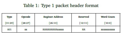
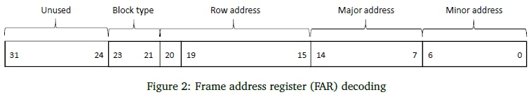
The physical position of each frame on the device is given by a unique 32-bit address. As shown in Figure 2, this address is divided into five parts, each relatively self-explanatory except for the minor and major addresses2. Each row of the FPGA is sub-divided into columns, addressed by using the major address. Each column corresponds to a block in the FPGA array and contains a certain number of frames. The address of each frame inside the column is addressed by the minor address.
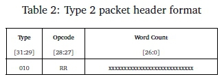
The configuration logic responsible for addressing the configuration memory consists of a packet processor and a set of registers and global signals with behaviour related to the content of the registers. The packet processor is responsible for the dataflow to and from the configuration memory, controlling the configuration process. Two types of packets are used to write to the configuration memory: Type 1, used for register reads and writes, and Type 2, for writing large blocks of data. Tables 1 and 2 show the format for each packet. The type of packet is indicated by the Header Type, the Opcode indicates a read, write or no operation and Word Count indicates the total number of words. A Type 1 packet also includes a Register Address indicating the type of register. For the method proposed in this paper, only three registers are of interest for parsing and analysing the contents of the bitstream: the frame address register (FAR), the frame data input register (FDRI), and the legacy output register (LOUT). The functionality of these registers are:
Frame Address Register (FAR) Specifies the address of the frame.
Frame Data Input Register (FDRI) Writes to this register configure frame data at the frame address specified in the FAR register.
Legacy Output Register (LOUT) Software uses this register to drive data to the DOUT pin3 during serial daisy-chain configuration. It is also used during debugging of the configuration.
For a detailed description of the configuration architecture, refer to the Xilinx® Virtex®-5 configuration user guide (Xilinx Inc., 2012).
4 BITSTREAM ANALYSIS METHOD
The method used to parse and analyse the bitstream is based on the technical report written by Castellone (2011). The general idea is illustrated in Figure 3 and involves:
1. Placing a base design created in Xilinx®'s FPGA Editor™ at the slice origin (SLICE_X0Y0). This design initialises all LUTs in the slice with zeros (0x0000000000000000), which implies a logical output of'0' for all possible inputs on A1 to A6. With the exception of the inputs and outputs of the slice, the rest of the design remains unrouted.
2. Next, the same design is used, but this time the LUTs are initialised with ones (0xFFFFFFFFFFFFFFFF). This is equivalent to a multiplexer with an output of '1', regardless of input. A valid Boolean expression for a multiplexer with an output of An, irrespective of input, is (A1 + A2 + A3 + A4 + A5 + A6) * 0 + An.
3. The bitstreams of these two designs are then compared and the differences highlighted by placing "X"s in the bit-positions where the differences were detected, as shown in Figure 4. The matching lines were converted into their equivalent hexadecimal values and decoded into a packet command.
4. Using the three steps above, the slice is then moved across the FPGA floorplan and the translation between logical x and y coordinates and frame coordinates determined by analysing the FAR-value of each slice.
5. To determine the encoding for each possible LUT primitive, the steps above were repeated, but this time the LUTs were initialised as multiplexers, ROM, RAM, and shift register LUTs (SRLs).
Castagna (2008) used Python™ to generate FPGA Editor™ batch scripts for opening the base design, moving the required slice to a new location, modifying its contents, re-routing the design, and saving the modified netlist. UNIX command-line tools were then used to generate the bitstreams. Castellone (2011) showed how this method can be applied to parse and analyse the bitstream of a Virtex®-4 FPGA, but the method was never adapted for newer FPGAs. Complex LUT primitives, such as RAM, ROM and SLR, were also not considered.
The method proposed in this paper is consistent with that of Castagna and Castellone's, but MATLAB® was used to generate FPGA Editor™ scripts and to compare the bitstreams. A different FPGA, the Virtex®-5 (specifically the XCVFX70T), was used to allow validation of the proposed method and to compare the results obtained by Castellone for a different FPGA. The following complex LUT primitives were considered:
• 6-input SLICEL multiplexer
• 6-input SLICEM multiplexer
• Hexadecimal value stored in ROM
• 64 1-bit values stored in RAM (RAM64X1)
• 16 8-bit values stored in RAM (RAM16X8)
• 16 4-bit values stored in RAM (RAM16X4)
• 32 8-bit values stored in RAM (RAM32X8)
• A 16-bit value stored in a SRL (SRL16)
• A 32-bit value stored in a SRL (SRL32)
In order to simplify the comparison of the bitstreams, switches -b and DebugBitstream:Yes were used when generating the bitstreams. These create a slightly larger ASCII bitstream with the commands grouped into 32-bit words (Xilinx, Inc., 2011), and generate a bitstream where every frame is written in a separate packet. The current frame address register (FAR) is also written to legacy output register (LOUT) after each write to the frame data input register (FDRI). These values were used to determine how each frame is written to the configuration memory. To further isolate the LUT configuration bits, all CRC checks were disabled.
5 BITSTREAM PARSING RESULTS
This section presents the results when parsing the bitstream of the Xilinx® Virtex®-5 XCVFX70T FPGA. It is important to note that although these results are device specific, similar results can be obtained by applying the methodology discussed in Section 4 to a different device. Even though a Virtex®-5 FPGA was the only platform available for implementing the bitstream specialiser of Section 7, using FPGA Editor™ it can be confirmed that similar results can be obtained for any Xilinx® FPGA with a similar configuration architecture.
5.1 Address translation
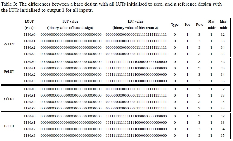
Figure 5 shows the typical result when comparing the base design, with all LUTs initialised with zeros, to a design with all LUTs initialised with ones. Each marker-set indicates the line in the bitstream where the differences were detected between the various LUTs, as well as the specific bits that differ. These differences are also tabulated in more detail in Table 3. In this table it can be seen that the 64-bits required to configure each LUT are equally distributed among four frames, as seen in the increase in minor addresses. In actual fact, it was found that the configuration of the 80 LUTs constituting a row of 20 slices are neatly contained inside four frames.
Combining this result with the information given in the configuration user guide for the device considered (in this case, the Virtex®-5 XCVFX70T (Xilinx Inc., 2012)), the content and composition of a single frame can be obtained. The result is shown in Figure 6 and contains the first 16-bit configuration data for each of the 80 LUTs in the 20 CLBs between (x, y) = (0,0) and (x, y) = (0,19). Also shown is the location of the 12 bits (bits 640 to 651) used to store the error checking code (ECC) for the frame, and the miscellaneous horizontal clock (HCLK) configuration bits (bits 652 to 655). Bits 656 to 671 are the unused HCLK configuration bits.
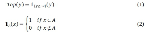
The FAR-values of each experiment were then used to derive a set of device-specific formulas to translate the slice coordinates to the frame address. For the Virtex®-5 XC5VFX70T FPGA, x = {0,1,...,75}, y = {0,1,...,159} and the LUTs are given by L = {A,B,C,D}. Because only block configurations are written, the block type will be set as Type = 0 (as per the configuration user guide (Xilinx Inc., 2012)) in each of the formulas. The top or bottom position, Pos, is given by (1), with 1 the indicator function defined by (2).
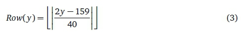
The height of the device considered is 159 slices with 40 slices per row. Because row numbering is repeated for the top and the bottom of the device, (3) is used to calculate the row.
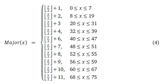
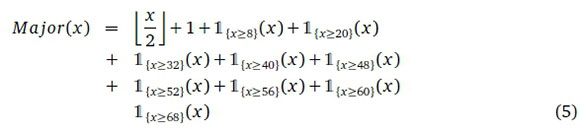
The derivation of the major address calculation, (4), was done by moving the slice horizontally across the FPGA floorplan. The offset added to each calculation is dependent on other columns, such as RAM, DSP and I/O, situated between the CLBs. Again, this equation can be simplified by using the indicator function as shown in (5).
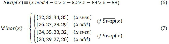
While moving the slice horizontally across the FPGA floorplan, an interesting phenomenon was observed; the configuration of every fourth column was byte-swapped. For even columns, the minor addresses [32, 33, 34, 35] were swapped to [34, 35, 33, 32] and for uneven columns minor addresses [26, 27, 28, 29] were swapped to [28, 29, 27, 26]. Castellone (2011) found that columns 30, 96 and 97 break this convention and also swap on the Virtex®-5 VLX110T. On the contrary, it was found that columns 50, 54 and 58 are swapped on the VFX70T. After further investigation, it was ascertained that these columns are SLICEMs on the respective devices. As a result, the byte swapping can be ascribed to a difference in encoding between SLICEL and SLICEM. Using this information, it is possible to determine whether the frame should swap using (6). In this Boolean equation, Swap is a binary variable that is only true if the bytes of the LUT configuration are permuted. From this, the composition and order of the minor addresses are given by (7).
5.2 LUT multiplexer encoding
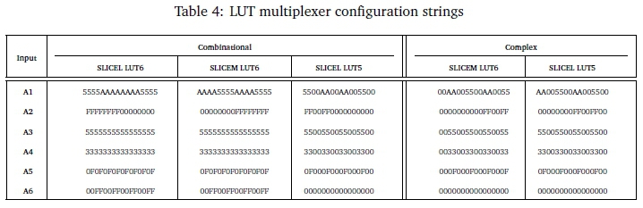
An η-bit LUT can encode any η-input Boolean function by modelling these functions as truth tables, with the columns corresponding to the inputs of the LUT. This is effectively the same as a multiplexer whose select lines are the inputs of the LUT, meaning that any η-bit LUT can be modelled as such. This is the fundamental hardware underlying any LUT primitive. By configuring the LUTs as multiplexers and comparing them to a base design, a unique set of 64-bit strings was found, listed in Table 4, used to encode the configuration data for each LUT input.
Listed under Combinational are the strings used to implement combinational logic on any slice type, whereas the strings listed under Complex are solely used to implement complex primitives, such as ROM, RAM and SRL, on SLICEMs. It is interesting to note that the configuration strings for the 5-input combinational logic are a subset of the 6-input configuration strings. This also holds true for complex memory primitives, because one input is controlled by software and as a result, only 5-inputs are used per LUT.
These strings can be used to derive the bitstream encoding of any LUT primitive by simply substituting each input variable into the Boolean expression represented by the LUT. Consider the following Boolean expression: A6LUT = ((A2 Λ (ATΛ (A3 Θ (A6 Θ (A4 ΘA5))))) V (A2 Λ (A1 V (A3 Θ (A6 Θ (A4 Θ A5)))))). By substituting the corresponding configuration strings into this equation, it is possible to show that the configuration for combinational logic implemented on a SLICEL and SLICEM would be 0x7DD7EBBE41142882 and 0x41142882EBBE7DD7 respectively.
5.3 LUT primitive encoding
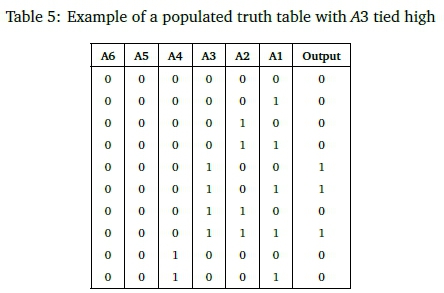
LUT primitives are described using a high level INIT-parameter. This parameter initialises the truth table for each of the LUTs in the slice. Consider an INIT-parameter of 0x00000000000000B0. Synthesizing this design and examining it in FPGA Editor, it is possible to analyse the placement and routing of the slice I/O. Say for instance that input A3 is tied high by the synthesiser. Using this information, the truth table can be populated as shown in Table 5 and because each entry in the truth table represents_a_Boolean function, this translates to (A6 Λ A5 Λ A4 Λ A3 Λ A2 Λ A1) V (A6 Λ A5 Λ A4 Λ A3 Λ A2 Λ A1) V (A6 Λ A5 Λ A4 Λ A3 Λ A2 Λ A1). Using the configuration strings in Table 4, the LUT configuration can be calculated as 0x4000400000004000 for SLICEM and 0x4000000040004000 for their SLICEL counterparts.
This also holds true for all LUT storage primitives. The only differences are the way the truth table is populated-the hardware is synthesised and optimised in different ways and the truth table is dependent on the LUT inputs-and the configuration strings used. Some control over the location and order of the LUT inputs can be exercised by adding placement and routing constraints, or by manual routing.
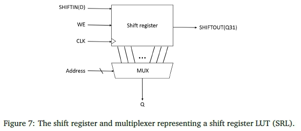
5.4 SRL encoding
The only variation to the LUT bitstream encoding occurs when considering SRL LUT primitives. This is because these primitives are represented by a shift register and a multiplexer, shown in Figure 7. Consequently, the SRL has an output, SHIFTOUT, for the most recent bit shifted out and an output, Q, where any of the bits in the register can be accessed. A dynamic read of the SRL is performed using the five most significant bits of the address lines (i.e. input A2 to A6). During this process, A1 is tied high. Therefore, every line in the truth table with A1 = 1 is used for initializing the output of the multiplexer (Q) and every other line is used to initialise the SHIFTOUT.
As an example, consider an SRL initialisation parameter of 0x0000000000000005. When inserting this value into a truth table for the SRL, only the lines with A1 = 1 are considered, as shown in Table 6. However, when calculating the Boolean expression represented by the truth table, the preceding lines should also be considered. This yields a Boolean equation of (A1 Λ A2 Λ A3 Λ A4 Λ A5 λ A6) ν (A1 λ A2 λ A3 λ A4 λ A5 λ A6) ν (AT λ A2 λ A3 λ A4 λ A5 λ A6) ν (AT λ A2 λ A3 λ A4 λ A5 λ A6).
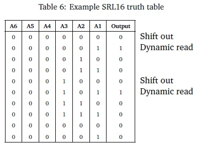
Again, using the configuration strings given in Table 4, this equation results in a configuration of 0xC000C00000000000.
6 PARSING AND ANALYSIS DISCUSSION
By comparing different reference designs to a base design, it was shown that it is possible to map the configuration space of the FPGA to the bitstream. In this instance, it was found that the Virtex®-5 XCVFX70T FPGA has its configuration of 80 LUTs equally spaced among four consecutive frames. Because 64 bits are required to configure a LUT, each frame contains 16 bits of the total LUT configuration. It was also shown that by analysing the FA.R-value of each packet in the bitstream, it is possible to derive a set of mathematical formulas for translating the device's slice coordinates to the frame address. This allows a designer to determine the exact frame address using the slice coordinates and protects from accidentally changing the bitstream content of an unknown component, creating hardware contention and potentially damaging the device.
To determine the specific device's bitstream encoding of the LUTs, different LUT primitives were analysed. The initialisation for each of these primitives is done using JMT-parameters, which initialises the truth table of the primitive and represents a Boolean expression. It was found that most of these can be modelled using multiplexers, and by analysing the bitstreams for each primitive configuration, it was possible to derive a set of configuration strings for both 5- and 6-input SLICEM and SLICEL slices. Using these derived configuration strings, it is possible to determine the bitstream encoding of any LUT primitive.
The modelling of SRL primitives differs from the other primitives mentioned above. This is because an SRL is modelled as a multiplexer with a shift register as input. It was found that in order to derive the Boolean expression represented by the SRL truth table for this device, the rows with A1 = 1 are used for initializing the multiplexer component and every other line is used to initialise the shift register. Once the Boolean expression is derived, the bitstream encoding can be obtained by applying the configuration strings.
The reason for focussing the results in Section 5 on the XCVFX70T, is because this device was used to implement the specialiser discussed in the following section. Despite this, the bitstream parsing and analysis method proposed in this paper is device independent and can be applied to any Xilinx® FPGA to extract certain characteristics. Generally, the differences between Xilinx®'s FPGA families' configuration architectures are; the frame length, the frame composition and the physical layout of hardware resources. Once these have been obtained for a new device, the methodology discussed in Section 4 can simply be applied for the new architecture. New formulas will then be derived depending on the frame length and composition, the homogeneity of the columns, and slice configuration.
This study was unfortunately limited by the toolset (which is considered deprecated), but similar results can be found for different devices in the Virtex® FPGA family up to the Virtex®-5. This is primarily due to these devices having similar configuration architectures. The Spartan®series FPGAs from Xilinx® have different configuration architectures, but with proper parsing and analysis, similar characteristics can be extracted.
Although FPGA Editor™ (which is part of the deprecated Xilinx® ISE® design suite) was used to parse and analyse the bitstream, it is possible to follow the same method using Xilinx®'s new VivadoTM design suite. The FPGA Editor™ scripts will be substituted by Tcl (Tool Command Language) equivalents, and the floor-plan centric nature of VivadoTM suits the proposed method perfectly. This approach is currently being investigated.
7 IMPLEMENTATION OF THE BITSTREAM SPECIALISER
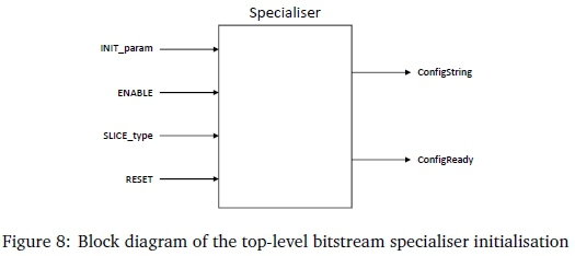
Figure 8 shows the top level block diagram of the developed specialiser. The specialisation process is triggered by a rising edge on ENABLE, whereafter the specialiser uses the new initialisation parameter (INIT_param) to produce a new configuration string (ConfigString) based on the LUT construct type (SLICE_type). The ConfigReady pin is used to establish handshaking with the rest of the hardware.
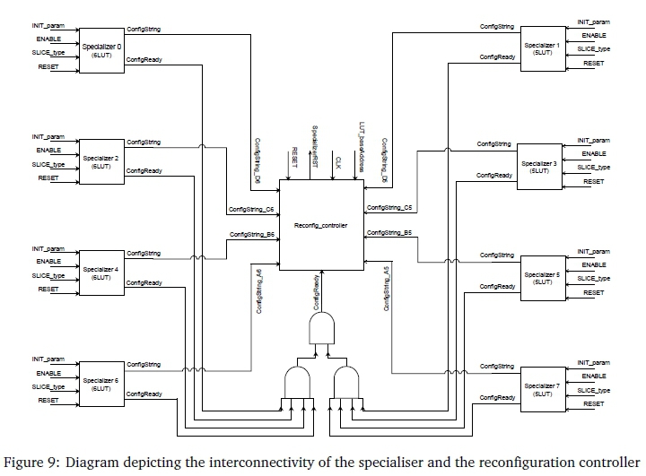
For this paper, an FPGA architecture was considered that combines four 6-input fracturable LUTs per slice (LUT5 and LUT6). Consequently, eight initialisation parameters are required to initialise each slice. This also implies that eight specialisers are required when implementing it in a system. The result is shown in Figure 9, with a reconfiguration controller as the hub of the process. This controller also encapsulates the internal configuration access port (ICAP) to transfer the new initialisation parameter to the configuration memory, and the state machine used for reconfiguration.
Also seen in Figure 9 is that the even-numbered specialisers are used to generate new configuration strings for the LUT6-expressions (ConfigString_A6 to ConfigString_D6), whereas the odd-numbered specialisers are used for LUT5 (ConfigString_A5 to ConfigString_D5). The AND-gates at the bottom of the figure use the ConfigReady signal of each specialiser to synchronise to the reconfiguration process. These lines are driven high once a valid configuration string is available. These strings are then injected into the bitstream at the address specified on LUT_baseAddress and transferred to the configuration memory by the reconfiguration controller. The injected words are done 16 bits at a time, corresponding to the location of the specific LUT in the bitstream. Once the reconfiguration process completes, a soft reset can be issued on SpecializerRST, should it be required.
8 VERIFYING THE SPECIALISATION PROCESS
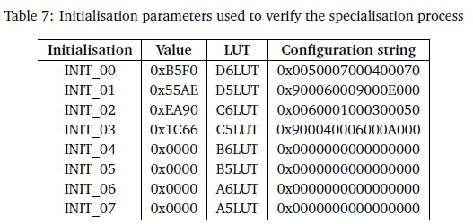
To verify the operation of the specialiser, consider a LUT primitive with the initialisation parameters and primitive listed in the first three columns of Table 7. Using a truth table a Boolean expression for each of the initialisation values can be derived. Next, the configuration parameters derived in Section 5 and listed in Table 4 are substituted into these expressions to yield the configuration strings given in the last column of Table 7.
As can be seen, these values correspond with the simulated results of Figure 10. Also seen in the figure is that the new configuration strings (ConfigString_D6 to ConfigString_A5) are available immediately after assigning the new initialisation parameters (INIT_param) and enabling the specialiser via ENABLE.
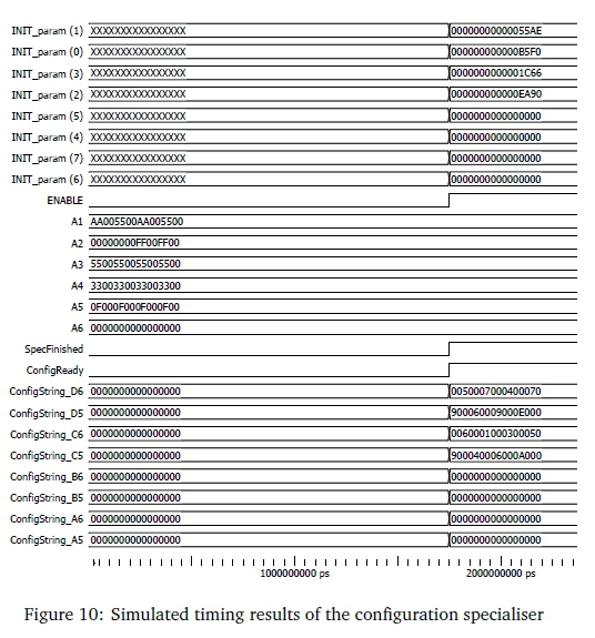
Figure 11 illustrates the timing of the reconfiguration controller using these values in the reconfiguration process. Once the specialisation process completes, the reconfiguration controller is notified using ConfigReady. A base configuration, also called the golden image which can be used for fallback, is then read from the memory, one word at a time, as shown by Configuration read and Word read, and sent to the configuration memory via the ICAP If the word counter matches the address specified on LUT_baseAddress (in this particular instance, 28), the corresponding configuration strings are injected into the current and subsequent line. This is repeated for every 41 words read, as per the frame composition. The Xilinx® reconfiguration user guide (Xilinx, Inc., 2010) also specifies that these values have to be byte swapped, which is shown by ICAP Input.
9 CONCLUSION
Despite the obscurity of the bitstream, this paper described a method used to parse and analyse the bitstream of a Xilinx® FPGA, based on work done by Castagna (2008) and Castellone (2011). Using this method, not only were mathematical formulas derived for translating the slice coordinates to frame addresses, but the configuration strings used to encode the LUT bitstream information for each slice were also extracted.
The general idea is that any LUT can be expressed as a truth table, with each line representing a Boolean function. The LUTs are initialised by a 64-bit4 initialisation parameter, which is used in conjunction with the address lines to determine the output of the truth table. This output is then encoded into a bitstream, with the specific encoding determined by the LUT primitive.
Using this information, it is possible to modify the configuration bits of a bitstream directly. Once the required LUT primitive is identified, the associated Boolean expression can be derived by using the initialisation parameter as an additional address line for its truth table. The Boolean expression is then evaluated using the configuration strings and the result placed into the bitstream at the required frame address.
This process was illustrated by implementing a bitstream specialiser in FPGA fabric. As a base bitstream is loaded from memory, a new configuration can be derived for the LUTs and injected into the bitstream while it is being transferred to the device's configuration memory via the ICAP This not only results in extremely high reconfiguration throughput without any latency, but also creates new hardware on-the-fly as required.
The implication is that a real-time system, such as the high-speed, five degree-of-freedom active magnetic bearing system developed in le Roux (2009), can be dynamically reconfigured regardless of its tight time constraints. An added benefit is an improvement in the functional density of the application. Functional density is a measure of the composite benefits of dynamic reconfiguration above its static generic counterpart, and measures the computational throughput (in operations per second) per unit hardware resources. Future work will include measuring this functional density advantage, as well as analysing the bitstream of a 7-series FPGA to see if similar characteristics can be extracted.
10 ACKNOWLEDGEMENTS
We thank Dr Fabio Cancaré for his willingness to share the methodology used by Davide Castellone (2011), which proved invaluable to our study.
This study was done under the Technology and Human Resources for Industry Programme (THRIP) and the Oppenheimer Memorial Trust Grant (Ref. 19328/01).
References
Beckhoff, C., Koch, D., & Torresen, J. (2011). The Xilinx Design Language (XDL): Tutorial and use cases. In 6th International Workshop on Reconfigurable Communication-Centric Systems-on-Chip (ReCoSoC) (pp. 1-8). https://doi.org/10.1109/ReCoSoC.2011.5981545
Benz, F., Seffrin, A., & Huss, S. A. (2012). Bil: A tool-chain for bitstream reverse-engineering. In 22nd International Conference on Field Programmable Logic and Applications (FPL) (pp. 735-738). https://doi.org/10.1109/FPL.2012.6339165
Blodget, B., James-Roxby, P, Keller, E., McMillan, S., & Sundararajan, P (2003). A self-reconfiguring platform. In P. Y. K. Cheung & G. A. Constantinides (Eds.), Field Programmable Logic and Application (pp. 565-574). https://doi.org/10.1007/978-3-540-45234-8_55
Bruneel, K. (2011). Efficient circuit specialization for dynamic reconfiguration of FPGAs (Doctoral dissertation, Department of Electronics and Information System (ELIS), Ghent University). Retrieved from http://www.iwls.org/iwls2013/invited/bruneel.pdf [ Links ]
Cancare, F., Santambrogio, M. D., & Sciuto, D. (2010). A direct bitstream manipulation approach for Virtex4-based evolvable systems. In Proceedings of 2010 IEEE International Symposium on Circuits and Systems (pp. 853-856). https://doi.org/10.1109/ISCAS.2010.5537429
Castagna, A. (2008). Progettazione di un sistema evolutivo hardware basato su Virtex-4 (Master's thesis, Politecnico di Milano). [ Links ]
Castellone, D. (2011). Analysis of the configuration bitstream format of a Xilinx Virtex-5 XCLX110T. Politecnico di Milano.
Celebucki, D., Graham, S., & Gunawardena, S. (2018). Reversing a Lattice ECP3 FPGA for bitstream protection. In J. Staggs & S. Shenoi (Eds.), Critical Infrastructure Protection XII (pp. 91-111). https://doi.org/10.1007/978-3-030-04537-1_6
Ciobanu, C. B., Stramondo, G., Varbanescu, A. L., Brokalakis, A., Nikitakis, A., Tucci, L. D., . . . Pnevmatikatos, D. (2018). EXTRA: An open platform for reconfigurable architectures. In Proceedings of the 18th International Conference on Embedded Computer Systems: Architectures, Modeling, and Simulation (pp. 220-229). SAMOS '18. https://doi.org/10.1145/3229631.3236092
Compton, K., & Hauck, S. (2002). Reconfigurable computing: A survey of systems and software. ACM Computing Surveys (CSUR), 34(2), 171-210. https://doi.org/10.1145/508352.508353 [ Links ]
Ding, Z., Wu, Q., Zhang, Y., & Zhu, L. (2013). Deriving an NCD file from an FPGA bitstream: Methodology, architecture and evaluation. Microprocessors and Microsystems, 37(3), 299-312. https://doi.org/10.1016/j.micpro.2012.12.003 [ Links ]
Ender, M., Swierczynski, I?, Wallat, S., Wilhelm, M., Knopp, P M., & Paar, C. (2019). Insights into the mind of a Trojan designer: The challenge to integrate a trojan into the bitstream. In Proceedings of the 24th Asia and South Pacific Design Automation Conference (pp. 112-119). ASPDAC '19. https://doi.org/10.1145/3287624.3288742
Guccione, S., Levi, D., & Sundararajan, P (1999). JBits: A Java-based interface for reconfigurable computing. In 2nd annual military and aerospace applications of programmable devices and technologies conference (mapld) (Vol. 261).
Horta, E. L., & Lockwood, J. W. (2001). PARBIT: A tool to transform bitfiles to implement partial reconfiguration of field programmable gate arrays (FPGAs). Dept. Comput. Sci., Washington Univ., Saint Louis, MO, Tech. Rep. WUCS-01-13. https://doi.org/10.7936/K7T43R9B
Kulkarni, A., & Stroobandt, D. (2016). How to efficiently reconfigure Tunable Lookup Tables for Dynamic Circuit Specialization. International Journal of Reconfigurable Computing, 2016, 3-14. https://doi.org/10.1155/2016/5340318 [ Links ]
Kusse, E., & Rabaey, J. (1998). Low-energy embedded FPGA structures. In Proceedings. 1998 international symposium on low power electronics and design (pp. 155-160). https://doi.org/10.1145/280756.280873
le Roux, R. (2009). An embedded controller for an active magnetic bearing and drive electronic system (Master's thesis, The school of electrical, electronic and computer engineering, North-West University). [ Links ]
le Roux, R., van Schoor, G., & van Vuuren, P (2015). Block RAM-based architecture for real-time reconfiguration using Xilinx FPGAs. South African Computer Journal, 56(1). https://doi.org/10.18489/sacj.v56i1.252 [ Links ]
Leonard, J., & Mangione-Smith, W. H. (1997). A case study of partially evaluated hardware circuits: Key-specific DES. In W. Luk, P Y. K. Cheung, & M. Glesner (Eds.), Field-Programmable Logic and Applications (pp. 151-160). https://doi.org/10.1007/3-540-63465-7_220
Morford, C. J. (2005). BitMat - Bitstream manipulation tool for Xilinx FPGAs (Master's thesis, Virginia Polytechnic Institute and State University). [ Links ]
Note, J.-B., & Rannaud, É. (2008). From the bitstream to the netlist. In Proceedings of the 16th international acm/sigda symposium on field programmable gate arrays (pp. 264-264). FPGA 08. https://doi.org/10.1145/1344671.1344729
Pham, K. D., Horta, E., & Koch, D. (2017). BITMAN: A tool and API for FPGA bitstream manipulations. In Design, Automation Test in Europe Conference Exhibition (DATE), 2017 (pp. 894-897). https://doi.org/10.23919/DATE.2017.7927114
Singh, Hogg, & McAuley. (1996). Expressing dynamic reconfiguration by partial evaluation. In 1996 Proceedings IEEE Symposium on FPGAs for Custom Computing Machines (pp. 188-194). https://doi.org/10.1109/FPGA.1996.564830
Stitt, G., Vahid, F., & Nematbakhsh, S. (2004). Energy savings and speedups from partitioning critical software loops to hardware in embedded systems. ACM Transactions on Embedded Computing Systems (TECS), 3(1), 218-232. https://doi.org/10.1145/972627.972637 [ Links ]
Swierczynski, P, Becker, G. T., Moradi, A., & Paar, C. (2018). Bitstream fault injections (BiFI) -Automated fault attacks against SRAM-based FPGAs. IEEE Transactions on Computers, 67(3), 348-360. https://doi.org/10.1109/TC.2016.2646367 [ Links ]
Swierczynski, P, Fyrbiak, M., Koppe, P, & Paar, C. (2015). FPGA Trojans through detecting and weakening of cryptographic primitives. IEEE Transactions on Computer-Aided Design of Integrated Circuits and Systems, 34(8), 1236-1249. https://doi.org/10.1109/TCAD.2015.2399455 [ Links ]
SymbiFlow Team. (2019). Project X-Ray. Retrieved from https://prjxray.readthedocs.io/en/latest/
Todman, T. J., Constantinides, G. A., Wilton, S. J. E., Mencer, O., Luk, W., & Cheung, P Y. K. (2005). Reconfigurable computing: Architectures and design methods. IEE Proceedings - Computers and Digital Techniques, 152(2), 193-207. https://doi.org/10.1049/ip-cdt20045086 [ Links ]
Upegui, A., & Sanchez, E. (2006). Evolving hardware with self-reconfigurable connectivity in Xilinx FPGAs. In First nasa/esa conference on adaptive hardware and systems (ahs'06) (pp. 153-162). https://doi.org/10.1109/AHS.2006.38
Xilinx Inc. (2012). Virtex-5 configuration user guide (User guide No. UG191). Xilinx Inc.
Xilinx, Inc. (2010). Virtex-5 FPGA configuration user guide (User guide No. UG191). Xilinx, Inc.
Xilinx, Inc. (2011). Command line tools use guide (User guide No. UG628). Xilinx, Inc.
Yu, H., Lee, H., Lee, S., Kim, Y., & Lee, H.-M. (2018). Recent advances in FPGA reverse engineering. Electronics, 7(10). https://doi.org/10.3390/electronics7100246 [ Links ]
Zhu, J., Li, Y., He, G., & Xia, X. (2007). An intrinsic evolvable hardware based on multiplexer module array. In L. Kang, Y. Liu, & S. Zeng (Eds.), Evolvable systems: From biology to hardware (pp. 3544). https://doi.org/10.1007/978-3-540-74626-3_4
Received: 17 Jul 2018
Accepted: 21 May 2019
Available online: 24 Jul 2019
1 Not according to scale
2 The major address is also referred to as column address
3 Serial data output for downstream daisy-chained devices.
4 For 6-input LUTs

