


Services on Demand
Article
 English (pdf)
 Article in xml format
 Article references
Indicators

Related links
-
 Cited by Google
 -
 Similars in Google
Share

 Permalink
R&D Journal
On-line version ISSN 2309-8988
Print version ISSN 0257-9669
R&D j. (Matieland, Online) vol.35 Stellenbosch, Cape Town 2019
http://dx.doi.org/10.17159/2309-8988/2019/v35a5
ARTICLES
A computational study on additively manufactured welding electrodes
D.M. KirkmanI; J. PillayII; J. PadayacheeIII
IDiscipline of Mechanical Engineering, University of KwaZulu-Natal (UKZN), South Africa, dan.m.kirkman@gmail.com
IIDiscipline of Mechanical Engineering, University of KwaZulu-Natal (UKZN), South Africa, joshuapillay2@gmail.com
IIIDiscipline of Mechanical Engineering, University of KwaZulu-Natal (UKZN), South Africa, PadayacheeJ@ukzn.ac.za
ABSTRACT
Advances in additive manufacturing technology present new design opportunities for metal parts that would otherwise be infeasible with subtractive manufacturing technologies. Clifford Machines & Technology (Pty) Ltd is an international producer of large mesh welding machines. The research was conducted with the aim of investigating the advantages that can be provided through the redesign of the mesh welding electrodes, for production using additive manufacturing. Simulation studies were applied in order to evaluate the performance of the redesigned electrodes and the results were compared to the existing electrodes. The results show that the electrodes designed for additive manufacturing achieved mass reductions of up to 58.2%. The electrodes were also able to support increases of current density by up to 98%, while operating at a lower temperature than the original electrodes. The study has identified the high initial cost of production and increased power consumption to be the disadvantages of additively manufactured electrodes.
Additional keywords: Additive manufacturing, mesh welding machines, copper electrodes
1 Introduction
Until recently, the design of mesh welding electrodes was constrained by conventional manufacturing processes that limited the geometry of parts to spaces which could be reached by machine tools. Direct Metal Laser Sintering (DMLS), and other emerging metal Additive Manufacturing (AM) technologies now provide a unique opportunity to improve the performance of metal parts that have approached the limit of performance optimization using conventional manufacturing methods.
Clifford Machines and Technology (Pty) Ltd [1] produces large mesh welding machines that make use of water-cooled electrodes to deliver the electrical current and press force required to weld wire mesh. This paper presents the results of a collaborative study between the University of KwaZulu-Natal and Clifford Machines & Technology (Pty) Ltd, on establishing the potential benefits of additive manufacturing of weld press electrodes.
The components of the electrodes that were redesigned for additive manufacturing included the electrode tip holders and insulation. Clifford Machines and Technology (Pty) Ltd desired a lighter electrode, with the aim of increasing the speed of the weld process. The objectives of the study were to redesign the upper and lower weld press electrode holders and the lower electrode riser, while using the new design opportunities presented by additive manufacturing to:
• reduce the total number of parts in the electrode assembly;
• eliminate power losses due to electrical contact resistance at the interfaces of parts in the mechanical assembly;
• optimize the geometry of the electrodes for weight reduction;
• improve the transfer of waste heat away from the electrodes;
• reduce pumping head losses in the cooling channels of the electrodes.
The designs were validated using a number of computational tools including current density simulations and computational fluid dynamics. The results show that the re-designed electrodes have the potential to outperform the designs that are currently in production in terms of mass, fluid head losses and cooling performance. The main drawback of the additively manufactured electrodes was found to be an increase in predicted power consumption due to higher electrical resistance.
2 Additive Manufacturing with Copper
A study was conducted by Dyer [2] on additive manufactured copper electrodes for a resistance welding machine. The study used a Selective Laser Melting (SLM) process with a 200 W laser to create the electrodes out of AcuPowder 150A. The study reported that the density of the electrodes reached 68.9% of the parent material after being post-processed via sintering. The water cooling circuits were not watertight and the porosity of the electrodes increased the power required to complete a weld by 15%. The density and porosity of laser sintered copper parts were also of interest in this study as the electrode holders would be required to conduct electricity and dissipate heat via cooling channels. A number of factors have been identified as having a significant influence on the density and quality of parts.
Tang et al. [3] conducted research on the effect of varying process parameters on the characteristics of direct laser sintered copper parts. The research reported that increased laser power, combined with a decreased laser scan spacing and scan speeds lead to higher density copper parts. The study also reported that increased laser power resulted in a decrease in the accuracy of parts but an improvement in the quality of the surface finish.
Balling is an effect that describes the coalescing of molten metal instead of forming a uniform melt track. Wettability refers to the ability of the laser-melted powder to spread on, and adhere to the underlying substrate. Balling occurs when the molten liquid does not adequately wet the underlying substrate [4]. Balling creates unfavourable defects and is a hindrance to achieving full material density in laser sintered parts. The balling effect is a severe impediment to subsequent powder deposition and causes defects such as porosity and increases the likelihood of delamination [5].
Copper electrodes have been produced by additive manufacturing methods, particularly DMLS, for application in Electrical Discharge Machining (EDM). Although this research is concerned with welding electrodes, the research into the production of EDM electrodes contains lessons in producing high density copper parts. A study conducted by Leong et al. [6], discovered that increased weight percentages of nickel in the copper powder matrix decreased the porosity of parts due to improved wettability and reduced balling effect of the copper-nickel powder. Vinod and Srinivasa [7] have also confirmed the favourable effects of nickel on improving part density and reducing porosity. A study by Amorim et al. [8] produced EDM electrodes via DMLS, using a metal-matrix of molybdenum and a copper-nickel alloy. The results showed that the electrodes with added molybdenum had superior durability against electric spark erosion.
Studies on additive manufactured copper and copper alloys have shown that these materials have a lower power absorption of laser radiation. Presently, DMLS is only suited to copper alloys as pure copper reflects up to 90% of the laser radiation [9]. The high reflectivity and high heat conductivity of copper and copper alloys has a significant adverse effect on obtaining dense copper parts. The absorptivity of infrared light by the material is also known to increase as it melts, leading to an unstable melt. A study conducted at the Fraunhofer Institute for Laser Technology (ILT) [10] made use of a 1000 W laser instead of a conventional 200 W laser, and the results showed that part density approached 99.9% of the density of the parent material. Nevertheless, the high levels of reflected laser radiation are detrimental to the additive manufacturing equipment.
A pure copper sintered electrode would be more attractive as it would be more electrically and thermally conductive than a copper alloy. Scientists at Fraunhofer ILT are presently developing a 400 W laser that is able to emit green laser light of wavelength 515 nm [11]. The absorptivity of copper at this wavelength length is expected to be considerably higher and the laser is expected to be more precisely focused, allowing the creation of complex, high accuracy parts.
Lodes et al. [12] reported producing samples of additively processed 99.94% pure copper powder via Selective Electron Beam Melting (SEBM). The advantage is that the energy transporting beam is not reflected by the surface as in DMLS. The study demonstrated that samples of 99.95% density could be produced at scan speeds of up to 3000 mm/s. A further advantage of SEBM is that minimal residual stresses remain in the part due to the high process temperature. However, DMLS is known to produce parts with higher accuracy and better surface finishes. DMLS is capable of producing dense parts with a typical accuracy of ±0.02-0.05 mm/25mm at build speeds of 5-20 cm3/h, with average surface roughness values varying from 4-10 μπι [13-14]. DMLS was assumed as the manufacturing method in this study.
3 A Review of the Existing Electrodes
Figure 1 below shows the upper and lower electrode assemblies on the mesh welding machines produced by Clifford Machines and Technology (Pty) Ltd. Each electrode assembly consists of a conducting electrode holder and modular, replaceable electrode tip. The lower electrode is separated from the "riser" by Tufnol grade 10G/41 insulation [15]. The geometries of these parts conform to traditional machining processes for the creation of the cooling channels and mounting features. The focus of the study was on the redesign of the electrode tip holders as these parts play a significant role in the efficiency of the machines.

The electrode tip dimensions are 90x20x20 mm. The upper electrode assembly, which moves during the operation of the mesh welding machine has a mass of 3.90 kg. The lower electrode and electrode riser assemblies, which remain stationary, have masses of 5.58 kg and 6.87 kg respectively. Brocadur® CCZ, DIN 2.1293 copper alloy is used for the electrode holders. The thermal conductivity of CCZ alloy is 320 W/mK and the electrical conductivity is 47 MS/m [16]. Brocadur® CCNB, DIN 2.1285 is used for the electrode tips with a thermal conductivity of 250 W/mK and electrical conductivity of 28 MS/m [16].
The upper and lower electrode holders and the riser make use of round water-cooling channels of 8.6 mm diameter. The channels are produced by drilling holes at right angles and plugging selected holes, either with solder or with screw-in plugs. Cooling water is circulated at a rate of 2 l/min. The electrodes require current to be supplied at a maximum of 12 kA at 60 Hz and 12 V.
4 Re-Designed Electrodes for AM
4.1 AM Material Selection
A commercially available, patented DMLS compatible material called RS-Copper was identified as the material of choice for the design study. It is available from PROTIQ GmbH, a subsidiary of Phoenix Contact GmbH & Co. KG. The material achieves a laser processed density of 8.82 g/cm3, which is 99.95% the density of pure copper [17]. The electrical conductivity of the material after heat treatment varies from 32 MS/m up to 50 MS/m. The thermal conductivity of the RS - Copper is 265.482 W/mK. The average surface roughness of parts is 8-9 μπι after sand blasting. The tensile strength and hardness of the material reaches 219 ± 10 MPa after heat treatment, making it suitable for the weld press application. PROTIQ GmbH successfully demonstrated the use of the material in a collaboration with Altair Product Design Inc., where the RS-Copper was used in developing geometrically optimized copper induction elements [18].
Electrodes manufactured by additive manufacturing can be complex in shape, requiring customized insulation. Nylon is appealing for electrical insulation due to its resistance to abrasion, high dielectric strength and volume resistance. Li et al. [19] conducted tests on Nylon 12 samples to characterise the AC breakdown strengths and volume resistivity. The effects of anisotropy on 3D printed insulation were investigated by using 1 mm thick samples, at 0.1 mm per laminate layer. The insulation was printed parallel and perpendicular to the electric field. The results of this investigation showed that the AC dielectric breakdown strength of Nylon 12 insulation printed parallel and perpendicular to the field were 23.52 kV/mm and 34.85 kV/mm respectively. The material was therefore deemed suitable for the weld press application.
4.2 Design Procedure
The focus of the study was on improving the design of the upper and lower electrode holders and the lower electrode riser. All three components required design for welding current transmission and water cooling. Each of the components requiring cooling had a significantly different topology, placing different constraints on cooling channel designs. The redesigns were constrained by the requirement that the new parts should be capable of interfacing with an existing weld press, weld strap and dovetail joint. The designs were also constrained for DMLS printing in a 250x250x200 mm build volume.
During operation, the components are not subject to mechanical stresses that are significant with regard to the mechanical properties of the material. The redesign procedure was therefore guided by the capabilities of DMLS as an additive manufacturing technology. The highest design priority was the mass reduction of components while preventing the components from overheating. The smoothing of current density to eliminate spots of high localised heating was also pursued in the design.
An iterative design process was adopted as follows:
1. Merge the interfaces of sub-components in the original components to create single components.
2. Perform a current density simulation on the original parts to identify zones of high and low current density.
3. Remove material by adjusting the part geometry in zones of low current density.
4. Eliminate current concentrating features in regions of high current density.
5. Repeat current density simulations on parts with modified geometries and examine the results. If the predicted current densities are tolerable proceed to step 6, otherwise repeat step 4 before proceeding.
6. Perform heat transfer simulations to identify hot spots. Examine the pressure head losses in the cooling channels.
7. Adjust the location and profile of cooling channels to be as close to areas where higher temperatures persist and to reduce head losses.
8. Repeat current density and heat transfer simulations to examine the impact of cooling channel profile on current density and thermal efficiency. If the predicted current densities are tolerable proceed to step 9, otherwise repeat steps 6-7 before proceeding.
9. Evaluate resulting geometries in terms of additive manufacturing constraints such as maximum overhang angle and hole diameter for the minimisation of support material and post processing. If design is infeasible, repeat steps 3-8.
10. Examine the weight of the components and if further improvement is possible, repeat steps 3-9, otherwise accept the design.
The significance of step 1 is that it exploits the advantage of additive manufacturing, where assemblies that previously consisted of 2-4 parts can now be manufactured as a single part. Converting assemblies into a single part eliminated contact resistance losses and localized heating at the conducting interface. The procedure documented in steps 1-9 was repeated twice before arriving at the final designs which are now presented in sections 4.3-4.4.
4.3 Upper Electrode Holder
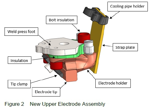
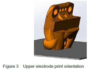
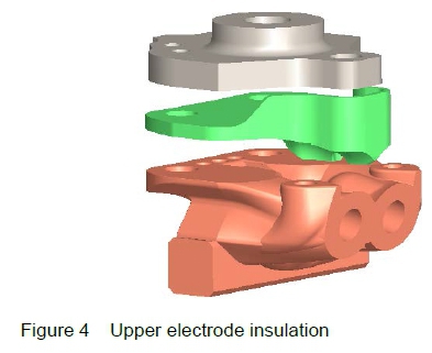
Figure 2 shows the redesigned upper electrode holder, assembled with the electrode tip, weld press foot, strap plate and various connectors. The final geometry and manufacturing orientation is shown in figure 3. The ends of the weld strap attachment bolt holes were tapered at 45° to prevent the need for support in these holes. Surfaces were angled relative to the horizontal so as not to require support. The part was designed to be cut from the build plate using wire EDM, resulting in a smooth contact surface with the weld strap plate. The electrode tip contact surfaces require machining and the holes for screw-in cooling channel inserts require drilling to improve surface finish and ensure dimensional accuracy. Figure 4 shows the electrode insulation topology (shown in green), which was designed to conform to the non-uniform shape of the electrode holder. The insulation could be injection molded, however 3D printing presents a clear advantage for lower quantities, as is the case at Clifford Machine and Technology (Pty) Ltd. The critical thickness of insulation assuming the absence of defects and moisture is 3.43x10⁻⁴ mm. A minimum practicable thickness of 4 mm was chosen for all insulation, which provided a large safety factor with respect to the ideal dielectric strength. The large safety factor accounts for the possibility of water absorption and arcing across the edge of the insulation. Tufnol grade 10G/41 (shown in red in figure 2) was used as in the previous design, in order to prevent arcing from the bolt to the electrode.
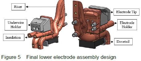
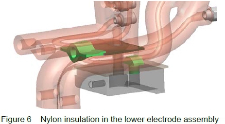
4.4 Lower Electrode Holder and Riser
The final design for the lower electrode assembly is illustrated in figure 5. Both the holder and riser were designed for DMLS, with the parts being orientated on their side for manufacturing. This orientation minimises the support structures that will be required. Insulating sheets used to separate the dovetail joint from the riser and the riser from the electrode holder were redesigned to accommodate the new shape of the electrode holder and single bolt for clamping the parts together. The material used for the insulating sheet was a phenolic paper laminated plastic that has the required insulating properties to separate the electrically conducting components as well as the strength and rigidity to withstand the forces exerted by the press during welding. An additional set of 3D printed nylon insulation was used between the dovetail joint and riser, and the electrode holder and riser in order to prevent the rotation
5 Current Density Simulations
Electric current density simulations were performed on STAR CCM+ to investigate the flow of current through the electrode holders and riser. The simulation allowed for the current density to be observed in order to predict potential "hotspots". The interaction of current with the cooling channel geometry, holes, and bends influenced the design of parts for electricity conduction. The cooling channel designs were iteratively adjusted to extract heat from areas that were expected to experience high localized heating. In areas of low current density, material was removed to reduce the weight of parts.
A maximum current of 12 kA was used to determine the current density at a voltage of 12 V across the circuit. Current flow was defined in simulations by specifying voltage and current boundary conditions on the surfaces corresponding to electrical connections, such as the strap attachment and electrode tip attachment surfaces for the upper electrode. The 'split by patch' function of Star CCM+ was used in defining surfaces bounded by closed curves, for the selection of surfaces to which boundary conditions were applied. A Surface Remesher was used for accurate analysis at the walls of the parts. A Polyhedral Mesher was used to create numerous polyhedral cells that occupy the volume of the model. A Prism Layer Mesh was used at walls of curved geometry. For the redesigned upper electrode, a cell size of 0.4 mm was used for the solid region, with the number of cells totalling 469 108. For the redesigned lower electrode, 540 188 cells were used with a base size of 0.65 mm. The physics models chosen to activate the current density simulation were: Three Dimensional, Steady, Solid, Electromagnetism and Electrodynamic Potential.
The electrical conductivity in the simulations was defined as 46.4 MS/m, which is achievable by the RS-Copper after heat treatment. The value was also selected for the study as it is comparable to the Brocadur® CCZ copper. This assumption allowed the merits of the original and revised designs to be compared with regard to part topology.
Figure 7 presents a sample current density simulation on the original upper electrode holder for reference. Figures 8-10 present current density simulations on the redesigned upper and lower electrodes, as well as the electrode riser. As anticipated, current concentrations appeared close to bends, holes and irregular shapes in the geometries.
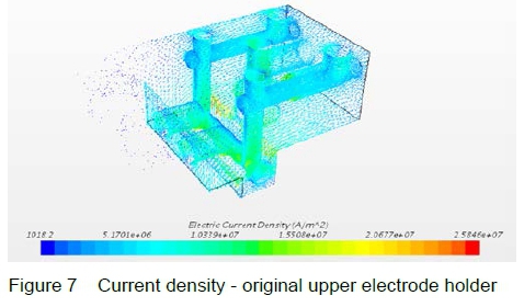
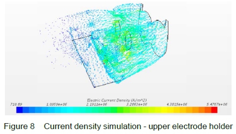
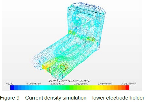
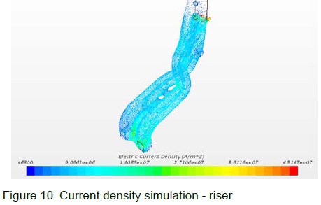
Reducing electrode mass was a higher design priority than reducing the average current density and electrical resistance. In many instances, the average current density increased due to the reduced mass of the electrodes; this was compensated for by improved cooling channel designs. The results of the simulations are summarised in table 1. The average current density simulations on the revised upper and lower electrode holder designs indicated increases of 97% and 88% respectively. The average current density of the lower electrode riser decreased by 8%.
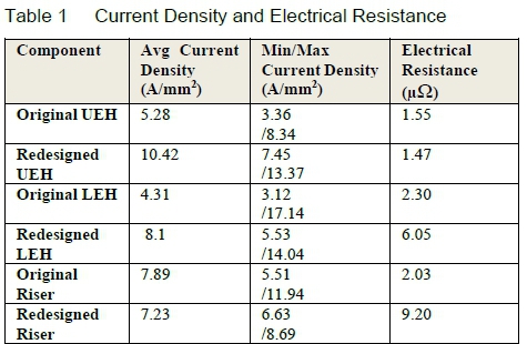
The electrical resistance of the lower electrode holder increased by a factor of 2.6 and the resistance of the riser increased by a factor of 4.6. The increase in resistance was due to a significant reduction in mass and cross sectional area of components. Furthermore, the original electrode holders and risers consisted of 2-3 components. Contact resistance losses between the conducting interfaces were not considered in the simulations.
Janiszewski and Ksiazkiewicz [20] place the contact resistance for a pure Cu-Cu, high quality surface contact at 2χ10-6 Ω, at a clamping force of 1000 N. The contact resistance for a CuCr25-CuCr25 contact was also experimentally found to be in the region of 2χ10-6 Ω, at a clamping force of 1000 N, with no significant improvement at higher clamping forces. If contact resistances are factored into the results as resistors in series, a more realistic prediction of the increase in electrical resistance of the lower electrode holder is a factor of 1.41 and the resistance of the riser increases by a factor of 1.52.
6 Cooling Investigation
6.1 Model Set-Up
Cooling is critical in keeping electrical losses to a minimum and in preventing the over-heating of the electrode. The advantages of the design flexibility provided by AM when designing the cooling channel arrangement was investigated by simulation. The cooling channel arrangements presented are not possible with conventional manufacturing technologies.
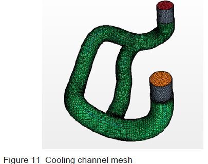
Two regions were created for the cooling channels and the electrode holder with tip attached. The solid regions made use of the meshes described in Section 5. The cooling channels used a polyhedral mesh with a prism layer mesher and surface remesher. A polyhedral mesh was used for the cooling channel region to adequately capture the convergence and divergence of flow which occurs in the manifold-type geometries of the redesigned cooling channels. A base size of 0.4 mm was used, along with volumetric controls at regions of significant curvature, using a base size of 0.16 mm for the redesigned upper electrode. The cooling channel mesh for the redesigned upper electrode consisted of 525 808 cells, while the corresponding mesh for the redesigned lower electrode consisted of 1 640 412 cells. Figure 11 shows the polyhedral mesh and interface on the cooling channel mesh for the redesigned upper electrode. The input, output and channel walls were specified as separate regions.
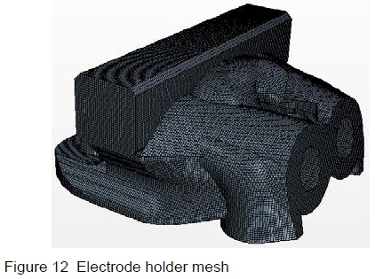
The electrodes used a trimmer mesh with surface remesher. A trimmer mesh was appropriate for heat transfer and electric current flow which occurs in the solid electrode holder region. The tip weld surface and electrical contact points were specified as separate surfaces for the application of boundary conditions. Figure 12 shows the trimmer mesh used for the electrode holder.
An initial simulation was performed to determine head loss through the cooling channel, and to compare this to the head loss through the original electrode holder design. The flow rate in both cases was 2 l/s. The push-in pipe fittings which attach to the electrode were included in the simulation. The simulation models were steady state, with constant fluid density. The standard k-ε model with high y+ wall treatment was appropriate for describing turbulent behaviour with heat transfer. The simulation was set-up as a coupled flow model to include heat transfer, together with coupled energy for the coupling of the solid and fluid models. Water was used as the cooling fluid and the effects of antifreeze were not considered.
The water inlet temperature to the electrode holders was set to 291 K, at a velocity based on channel diameter such that a flow rate of 2 l/s was obtained.
6.2 Heating Model
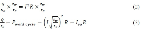
The Joule Heating model of Star CCM+ was used to evaluate heat dissipation through the resistance of the electrode holder components. A steady state (continuous) weld current value was required in order to approximate the periodic pulses of weld current if a steady analysis was to be conducted. During welding, weld current I is applied for a weld time tw. The total cycle time tcis the time for the press to complete a full cycle. It should be noted that current values are RMS values. The power dissipated while the weld current is applied is given by equation (1):

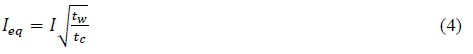
Here, Qperweid is the heat dissipated per weld cycle and R is the effective resistance of the electrode holder. Root-mean-square alternating current is defined as the ""steady (DC) current which when flowing through a given circuit for a given time produces the same heat as produced by the alternating current when flowing through the same circuitfor the same time" [21]. An equivalent RMS current value, Ieq, had to be obtained for I such that Ieqdissipated the same amount of heat when applied over the total cycle time tc as the heat generated by the weld current I flowing during the weld time. The value of Ieq was obtained by applying the heat dissipated by the weld over the entire weld cycle time instead of the weld time as follows:
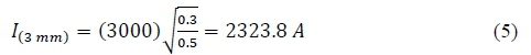
The equivalent steady-state value for weld current was therefore calculated from the weld and cycle times as follows:
On a mesh welding machine using 3 mm wire with weld speed of 120 crosswires-per-minute; the cycle time is 0.5 s, the weld time is 0.3 s and weld current is 3 kA. Thus:
This current was applied as a boundary condition at the weld strap attachment point of the upper electrode holder. The voltage at the tip surface was set to 12 V, while all other surfaces of the electrode and electrode tip were defined as electrical and thermal insulators. A heat flux of 332 W was applied at the electrode tip welding surface to simulate the average heat generation during the weld process.
The heat flux applied at the tip surface was approximated from the heat dissipated by the flow of 2323.8 A of current through a steel wire of diameter and length 3 mm. A resistivity of 1.45x10⁻⁷ Ω/m was used, which corresponds to the resistivity of low alloy steel wire [22].
The models included the following elements: coupled solid energy, electromagnetism, electrodynamic potential and ohmic heating. The electrode and riser material properties were specified in sections 3-4. Surface resistance at electrical connections was ignored, and the electrode tip was assumed to have the same properties as the holder.
6.3 Cooling Simulation Results
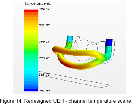
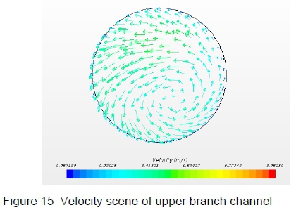
Temperature scenes for the upper electrode holder are shown in figures 13-14. The design made use of a parallel cooling channel arrangement as shown in figure 14. This arrangement facilitated the cooling of regions in close proximity to the surfaces which contact the electrode tip. The diameter of the parallel regions ranged between 6 - 7 mm, while the single regions have a diameter of 7 mm, being suitable for manufacture by DMLS. The branches were lofted from the single regions such that they were tangential at the point of splitting. Tangency reduces the head loss at the split and prevents "curtaining" effects where the branches join. Curtaining could result in a greater flow rate through one of the branches by causing resistance to flow from the other branch entering the join. Results of the head loss simulations, taking losses at the screw-in fittings into account, indicated an increase in head loss of 3.4% from 1870.6 Pa (191.0 mm) to 1934.9 Pa (197.0 mm) for the redesigned upper electrode channels. This slight increase was attributed to the use of narrower screw-in fittings which were chosen to avoid cracking of the electrode holder while tapping threads. The average flow velocity observed was slightly higher in the lower branch of the channel, indicating that the flow rate through this branch was greater than through the longer upper branch. The maximum temperature at the tip surface was 47.0 °C, which was 7 °C less than that on the original design. The side of the tip closest to the cooling channel input was at a lower temperature than the opposite side due to asymmetrical cooling. Significant whirl and secondary flows existed due to the channel bends, as illustrated in the velocity vector scene for the upper branch in figure 15.
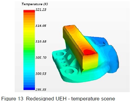
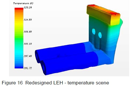
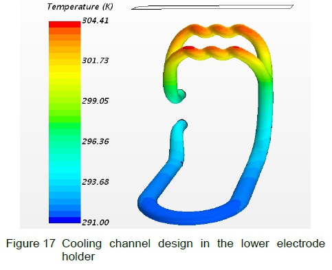
Temperature scenes for the lower electrode holder are shown in figures 16-17. The new lower electrode holder used a helical cooling channel design, as shown in figure 17, in order to utilise the cooling effects of secondary flows. Since the holder is now one piece, the cooling channel extends into the horizontal region of the L-shaped geometry. The heat transfer and fluid flow simulations conducted on the lower electrode yielded a pressure head loss in the cooling channel for the new design at 2597.9 Pa (264.8 mm), which is less than that of the old design which had a pressure head loss of 2720.7 Pa (277.3 mm). This indicates a 4.5% reduction in pressure head loss of the new lower electrode holder design. The maximum temperature at the electrode tip is 47.0 °C, as shown in figure 16, which is 11 °C less than the temperature achieved at the tip in the original design.
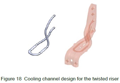
The cooling channel design for the new riser features a single continuous channel as compared to the two separate channels drilled into the blocks that previously made up the riser. From the head loss simulations conducted on the channels, a 44.69% reduction in head loss was observed from 3082.6 Pa (314 mm) down to 1705.0 Pa (174 mm) for the new channels thus verifying an improved design. Figure 18 below shows the cooling channel design for the riser.
7 Discussion
Load testing was performed on the weld presses manufactured by Clifford Machines & Technology (Pty) Ltd. Varying weights were placed onto the weld press to simulate the reduced weight of the AM electrodes. Tests at a constant pneumatic pressure, revealed that a weight reduction did not increase the speed of the weld press. Due to this observation and the estimated cost of manufacture using copper, plans to manufacture the redesigned electrodes via DMLS were suspended until the design of the weld press could be improved.
Due to the suspension of plans to manufacture the electrode components by DMLS, the upper electrode holder was investment cast in bronze as a fast and cost effective alternative. The investment casting required that the component was split into two parts. PLA models of the two parts were 3D printed. These models were then coated with a ceramic shell, and the PLA was burned out of the mold. Finally, the casting was performed, and the two parts of the electrode were soldered together. The investment casting shown in figure 19, served the purpose of demonstrating that the optimized geometry could be not be produced by conventional manufacturing methods as a single part. The investment casting also served to demonstrate the integration of the new design with an existing weld press.
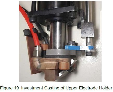
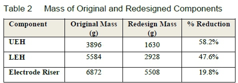
The investment cast electrode holder was not useful for testing as the bronze had significantly different electrical, surface finish and heat conducting characteristics. The design and simulation study provided promising results that AM electrodes have the potential to outperform the electrodes manufactured by traditional methods on a number of characteristics. The highest design priority was the reduction of the electrode holder and riser masses. The reduction in mass between additive manufacture and traditional designs is shown in table 2, where the quoted masses are the total masses that include fittings. The masses were determined by software estimation in the SolidWorks CAD environment. The results show that a mass reduction of up to 58% was achieved on the upper electrode holder.
The simulations revealed that the reduction in electrode holder mass increased the average current densities in the revised designs by up to 97%. The increase in current densities was compensated for by improved cooling channel designs, where both electrode holders and the electrode riser demonstrated a drop in temperature under the same operating parameters as the original design. The upper electrode holder demonstrated a slight increase in pressure head loss of 3.4%, while the lower electrode holder and riser demonstrated reductions in head loss.
It was noted that the electrical resistance of the lower electrode holder and electrode riser increased by estimated factors of 1.41 and 1.52 respectively. The increase in resistance leads to a proportional increase in power consumption, suggesting that the mass and cross sectional area of these components should be increased. It is important to note that only the upper electrode holder moves during a weld cycle.
8 Conclusions
The aim of this research was to explore the advantages that additive manufacturing could provide in the production of mesh welding electrodes. AM provides the advantage of complexity without additional manufacturing costs. Two mesh welding electrode holders and an electrode riser were redesigned for AM and compared, by simulation, to the original designs. The results show that AM is able to provide a clear advantage with regard to the mass reduction of components. Nevertheless, a trade-off exists, as current densities and electrical resistance increase as less material is used in the components. This leads to a higher power consumption by conducting components and additional waste heat being generated. AM allowed for the creation of complex cooling channels, which in turn aided in the improved removal of the waste heat.
In this research, only the upper electrode holder demonstrated a clear advantage in mass reduction, electrical resistance, and a reduction in operating temperature, via simulated results. In reality, these advantages may be further eroded by the ability to obtain high density copper parts via DMLS. Authors such as Dyer [3], reported a 15% increase in power consumption due to the porosity of the AM electrodes. Design optimization, advances in the laser sintering of copper, and the improved accessibility of the technology are the critical factors that will determine the industry success of additively manufactured copper electrodes in the future.
Acknowledgements
The authors would like to thank the University of KwaZulu-Natal (UKZN) and Clifford Machines and Technology (Pty) Ltd for supporting this research.
References
[1] Large Mesh Welders. URL www.cliffeng.com/large-mesh-welders.html, 2019.
[2] B.R. Dyer. Additive Manufacturing of Copper Electrodes and Bus Work for Resistance Welding. Master's thesis, Youngstown State University, USA, 2017. [ Links ]
[3] Y. Tang, H.T. Loh, Y.S. Wong, J.Y.H. Fuh, L. Lu and X. Wang. Direct laser sintering of a copper-based alloy for creating three-dimensional metal parts. Journal of Materials Processing Technology, 140(1-3):368-372, 2003. [ Links ]
[4] S. Das. Physical aspects of process control in selective laser sintering of metals. Advanced Engineering Materials, 5(10):701-711, 2003. [ Links ]
[5] Y.F. Shen, D.D. Gu and Y.F. Pan. Balling Process in Selective Laser Sintering 316 Stainless Steel Powder. Key Engineering Materials, 315:357-360, 2006. [ Links ]
[6] C.C. Leong, L. Lu, J.Y.H. Fuh and Y.S. Wong. In-situ formation of copper matrix composites by laser sintering. Materials Science and Engineering A. 338(1-2):81-88, 2002. [ Links ]
[7] A.R. Vinod and C.K. Srinivasa. Studies on laser-sintering of copper by direct metal laser sintering. In Proceedings: 5th International & 26th All India Manufacturing Technology, Guwahati, Assam, India, 12-14 December 2014.
[8] F.L. Amorim, A. Lohrengel, N. Müller, G. Schäfer and T. Czelusniak. Performance of sinking EDM electrodes made by selective laser sintering technique. International Journal of Advanced Manufacturing Technology, 65(9-12):1423-1428, 2013. [ Links ]
[9] Fraunhofer ILT Researching Green Lasers for 3D Printing Copper. URL 3dprint.com/186009/fraunhofer-ilt-3d-print-copper/, 2019.
[10] D. Becker and K. Wissenbach. Additive manufacturing of copper components. Fraunhofer ILT Annual Report, 2009.
[11] D. Heußen and S. Bremen. Green Light for New 3D Printing Process. Fraunhofer ILT Press Release, 30 August 2017.
[12] M.A. Lodes, R. Guschlbauer and C. Körner. Process development for the manufacturing of 99.94% pure copper via selective electron beam melting. Materials Letters, 143:298-301, 2015. [ Links ]
[13] I. Gibson, D. Rosen and B. Stucker. Additive Manufacturing Technologies: 3D Printing, Rapid Prototyping, and Direct Digital Manufacturing. Springer-Verlag, New York, 2nd edition, 2015.
[14] B. Langefeld. Additive manufacturing - A game changer for the manufacturing industry? URL www.rolandberger.com/publications/publication.pdf/rolandbergeradditivemanufacturing1.pdf, 2013.
[15] Tufnol Grades, m.tufnol.co m/tufnol-grade-10g-40.aspx, 2019.
[16] Brocadur Copper Alloys. URLwww.brouwermetaal.com/en/products/brocadur-copper-alloys.html, 2019.
[17] Protiq Material Datasheet-Laser Melting. URL www.protiq.com/out/pictures/ddmedia/PROTIQData heetLasermelting-EN.pdf, 2019.
[18] Highly conductive copper inductors from the 3D printer. www.protiq.com/pdfs/PROTIQHighlyconductivecopper-EN.pdf, 2019.
[19] Z. Li, H. Li, J. Rao, C. Yan, L. Li, F. Lin, Y. Liu and Y. Pan. Anisotropy on electrical insulation performance of 3D printed nylon 12. In: 2017 IEEE Conference on Electrical Insulation and Dielectric Phenomenon (CEIDP), Fort Worth, TX, USA, 22-25 October 2017.
[20] J. Janiszewski and A. Ksiazkiewicz. Vacuum switches contact resistance. Computer Applications in Electrical Engineering, 12:227-236, 2014. [ Links ]
[21] B.L. Theraja and A.K. Theraja. A Textbook ofElectrical Technology, S. Chand and Company PVT. Ltd., 2008.
[22] Conductivity and Resistivity Values for Iron & Alloys. URL www.nde-ed.org/GeneralResources/MaterialProperties/ET/ConductivityIron.pdf, 2019.
Received 4 June 2019
Revised form 28 October 2019
Accepted 5 November 2019

