


Services on Demand
Article
 English (pdf)
 Article in xml format
 Article references
Indicators

Related links
-
 Cited by Google
 -
 Similars in Google
Share

 Permalink
Journal of the Southern African Institute of Mining and Metallurgy
On-line version ISSN 2411-9717
Print version ISSN 2225-6253
J. S. Afr. Inst. Min. Metall. vol.114 n.2 Johannesburg Feb. 2014
PRECIOUS METALS CONFERENCE 2013
Structural and electrical characteristics of printed silver and palladium nanoparticle networks
C.B. van den BergI; M. TopicII; B. MagunjeI; D.T. BrittonI; M. HartingI
INanoSciences Innovation Centre, Department of Physics, University of Cape Town, Rondebosch, Cape Town, South Africa
IIMaterials Research Department, Somerset West
ABSTRACT
In this study, silver and palladium nanoparticulate inks with different metal-binder ratios were screen-printed onto a paper substrate. The printed layers comprised the metal nanoparticles and an ethyl cellulose binder. The layers are not typical metal composites due to the low concentration of binder and high porosity. The electrical sheet resistivity of each particle concentration was measured, and the data fitted using the scaling law of percolation theory and the general effective media (GEM) equation. The percolation parameters, i.e. the percolation threshold and the critical exponent, for each system were determined from the fits and compared. The percolation threshold for the palladium layer (39.8 wt%) was lower than that found for the silver layer (44.9 wt%). The critical exponents determined for the palladium and silver layers were both lower than the universal value for three-dimensional percolation systems. Microscopy observations indicate that the difference in the percolation threshold for the two layers can be attributed to variations in their microstructure.
Keywords: printed electronics, nanotechnology, nanoparticulate inks, silver, palladium.
Introduction
Printed electronics technology has attracted interest over the last few years as an alternative to conventional methods for the fabrication of electronic devices. Printing techniques such as screen and inkjet printing and gravure printing have been used for fabricating electronic devices. These techniques are advantageous because they are relatively simple, promise low production costs, and can be adapted for large scale production. Another advantage is the wide variety of materials, such as paper, plastics, and ceramics, that can be used as substrates (Britton and Harting, 2006; Faddoul et al., 2012). One of the major challenges is to formulate suitable inks for the different printing techniques. Functional electronics inks consist of nanoparticles (NP) dispersed in a liquid medium. Printing the inks involves the selectively deposition of the functional materials onto a substrate followed by a curing stage which may involve a number of processing steps (Britton and Harting, 2006; Shim et al., 2008). For this reason metallic NP are of particular interest due to their forming conductive tracks. Conductivity through the printed layer depends on how densely the NP are packed in the printed layer after curing (Shim et al., 2008). The final microstructure of the layer is also affected by the solvent and substrate used (Suvakov and Tadic, 2010). The basic requirement is therefore that the concentration of the NP must be above the percolation threshold for charge transport (Suvakov and Tadic, 2010). Conductivity through the material occurs through tunnelling or hopping of carriers and is influenced by factors such as the size and shape of the NP, composition, as well as the interparticle separation of the metal NP in the layer (Zabet-Khosousi and Dhirani, 2008; Sichel and Gittleman, 1982). In this study, silver (Ag) and palladium (Pd) nanoparticulate inks were produced with different metal-binder concentrations and deposited onto a substrate using screen printing. Percolation theory was used to determine the percolation threshold pc and the critical exponent of the layers. The nanoparticle shape and packing structure in the printed layers were studied using scanning electron microscopy (SEM). Observations made about the microstructure of the Ag and Pd layers are related to the percolation parameters obtained from the fits.
Percolation theory
Many properties of composites and colloid systems (i.e. electrical, mechanical, thermal, and optical) are determined by the distribution of the disperse phase in a dispersion medium (Vysotsky and Roldughin, 1999). Percolation theory has been used to understand changes in physical properties when transitioning from a disconnected to a connected structure in disordered systems (Nan, Shen, and Ma, 2010; Sahimi, 1994)
These physical properties include electrical resistivity and thermal conductivity of diphasic materials (McLachlan, 1990). Classical percolation theory deals with a lattice of 1, 2, 3, n-dimension that can be made up of a site or a bond which is randomly assigned with an occupation probability p (vacant, 1-p) (McLachlan, Blaszkiewicz, and Newnham, 1990; Leuenberger, 1999). In bond percolation, the cluster size depends on the number of bonds that connect neighbouring particles. In site percolation, cluster formation is a function of the occupation probability of the lattice chosen (Leuenberger, 1999). Lattice percolation is dependent only on the dimensionality and not on the properties of the lattice. Since most materials are heterogeneous (i.e. more than one phase), a continuum percolation will occur (Nan, Shen, and Ma, 2010). In this model the occupation probability p is replaced with a volume fraction of objects with a particular shape (Kirkpatrick, 1973). If one considers a system comprising two different particles with conductivities σ1 and σ2 respectively, such that σ2 « σ1, at very low concentrations of the high conducting particles, the lattice is insulating. Small particle agglomerates begin to form as the concentration of the more conducting particles is increased. As the concentration of the conducting particles is further increased, single conducting clusters begin to form. At a critical concentration of the conducting particles pc, known as the percolation threshold, conducting links are formed between single clusters, resulting in the formation of an infinite conducting cluster that spans the entire lattice. Therefore the conductivity of the system becomes finite. Above pc, the infinite cluster will incorporate additional small single clusters resulting in the increase in conductivity of the system (McLachlan, Blaszkiewicz, M., and Newnham, 1990; Leuenberger, 1999; Roldughin and Vysotskii, 2000) that can be described by the fundamental power law of percolation theory:

Here σ0 is the proportionality constant, p the volume fraction, and t the critical exponent. The power law holds only for values of p above pc (Kirkpatrick, 1973). The critical exponent t is said to be universal for 3D percolation systems, and dependent only on the spatial dimensions of the system. pc is affected by geometric parameters i.e. particle shape, polydispersity, and orientation (Roldughin and Vysotskii, 2000).
The problem in percolation theory is it assumes that a binary system below pc behaves as a perfect insulator (σi= 0). Above pc the conductivity of the system becomes infinite (σm = ∞) (McLachlan, 1990). To overcome this problem a general effective media (GEM) equation [2] has been proposed that takes into account the finite values for σi and σm above and below pc (McLachlan, Blaszkiewicz, M., and Newnham, 1990):
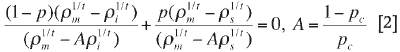
Here t is the critical exponent, p is the volume fraction of the conducting phase, pc is the critical volume fraction, pm is the resistivity of the system, and pi and ps are the resistivities of the phases with low and high conductivity respectively. The GEM equation is based on effective medium and percolation theories. The advantage of the GEM equation is that it has the same parameters (pc and t) that are used in percolation theory (McLachlan, Blaszkiewicz, and Newnham, 1990; McLachlan, 1990).
Experimental procedure
Sample preparation
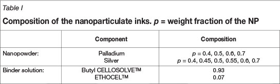
The palladium (Pd) NP were supplied by MKNANO and the silver (Ag) NP containing PVP dispersant was supplied by Sigma-Aldrich, Steinheim, Germany. Inks were prepared using ethyl cellulose (ETHOCELTM, Dow Chemical Company) as binder and Butyl CELLOSOLVETM acetate (Dow) as the solvent. Nanoparticulate inks were prepared with different metal-binder ratios as shown in Table I. The nanoparticulate inks were printed using an ATMA AT-60PD semi-automatic flatbed screen printer (Suvakov and Tadic, 2010). Screens made from monofilament polyester fibre with a mesh count of 150 lines per centimetre (supplied by Register Screen (Pty) Ltd) were used for printing. The samples size was 1x1 cm with a thickness of approximately 15-20 µm. The thickness of the layers was determined using a Veeco NT9100 optical profiler operating in the vertical step interferometry (VSI) mode. Plain white 80 g/m2 density paper, with no pre-treatment, was used as the substrate. The prints were allowed to cure for at least 48 hours under ambient conditions.
Morphological and electrical characterization
The shape, crystallinity, and size of the NP were observed with a JEOL JEM-2100 transmission electron microscope. The microstructure of the printed layer was investigated by SEM using a FEI Helios Nanolab 650 FIB-SEM operating in the single electron mode. Only the SEM feature was used for imaging the surface of the layers. The electrical properties of the printed metallic layers were measured using the LakeShore 7500 Series Hall Effect Measurement System. The sample was mounted onto the sample card and the probes placed at each corner. The quality of the contacts was assessed by measuring the I-V curves between pairs of contacts. The electrical sheet resistivity ps was measured in the van der Pauw geometry, which uses four contacts in a square configuration. A sweeping current was applied and the voltage between contacts measured (LakeShore Cryotronics, n.d.). The ps data was plotted as a function of the particle weight fraction instead of the volume fraction because the volume that the nanoparticle-binder mixture occupies is not easily quantified due to the high surface roughness of the paper substrate. All measurements were performed at ambient conditions.
Results and discussion
Morphology of the NP and printed layers
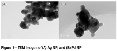
Transmission electron micrographs of the metal powders (Figure 1) detail their polydispersed nature. The size of the NP varied between 50-100 nm for Pd and 20-50 nm for Ag. The Ag NP were spherical or slightly elongated, whereas the Pd NP were multifaceted.
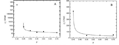
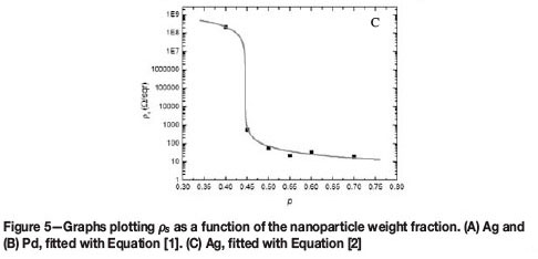
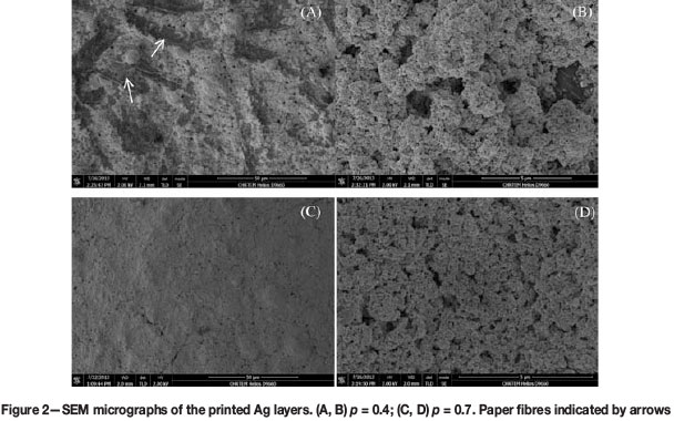
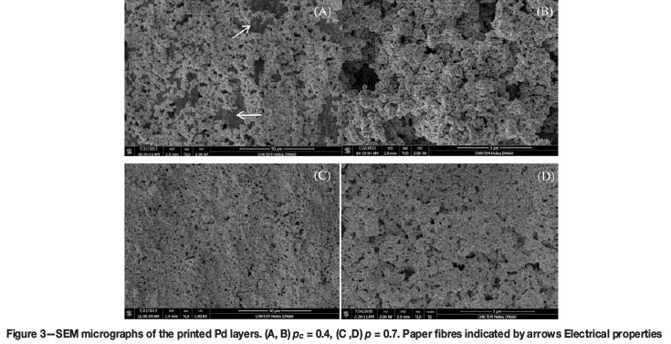
Figures 2 and 3 show the SEM micrographs of printed Pd and Ag layers for particle weight fractions of 0.4 and 0.7. The printed layers are not typical metal composites in the sense that they are not a dense material comprising a reinforcing phase (particles) embedded in a matrix phase (polymer, ceramic). Our layers consist of the metal NP, the polymer binder, and voids left after the solvent has evaporated. The voids represent regions that are insulating for an electron current passing through the layer. There is a change in the microstructure above and below pc for both metallic layers. At low particle concentrations the NP aggregate to form small defined clusters. As the concentration is increased, the clusters become larger as smaller neighbouring clusters are incorporated. At high particle concentrations an almost uniform layer is formed. It can also be observed that the clusters of the Pd and Ag NP are structurally different. At a low particle concentration of p = 0.4, the Ag NP aggregate to form a more compacted packing structure that fills the regions between the paper fibres (Figure 2A), resulting in 'isolated silver clusters' separated by the paper fibres. The Pd layer shows a high degree of porosity at both low and high particle concentrations (Figure 3). The Pd NP aggregate to form 'chain-like' structures that extend over the paper fibres. The observed differences in the microstructure could be due to the presence of the dispersant in the Ag ink, which is not present in the Pd ink. This may affect the clustering of the particles during ink production and the printing process. Furthermore, the distinguishing features in the shapes of the particles can result in differences in their surface energies, and thus a variation in the way they cluster.
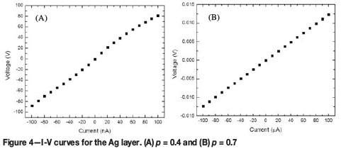
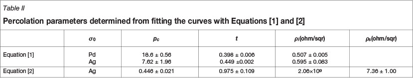
The I-V characteristics of the printed layers show ohmic behaviour for all particle concentrations, except for p = 0.4 of the Ag layers, which displayed nonlinear behaviour (Figure 4). Above pc the nanoparticle clusters aggregate to form a continuous particle network that extends throughout the layer. Therefore the conductivity of the layer is expected to approach that of the bulk metal. Below pc the clusters become isolated, resulting in fewer conducting paths. As a result, the conductivity of the layer deviates from the expected metallic behaviour (Zabet-Khosousi and Dhirani, 2008). Figure 5 shows the sheet resistivity ps plotted as a function of the particle weight fraction. It is observed that the ps increases as the particle concentration is decreased. The ps of the Ag layer increases rapidly from 400 ohm/sqr to 200 ohm/sqraround a critical particle concentration of between 0.4-0.45 (Figure 5A). A smaller change in the ps is observed in the Pd layers in the region of p = 0.4-0.5 (Figure 5B).The value of pc will therefore lie somewhere in the concentration range. The percolation parameters, pc and t, were determined from fitting the ps data with Equations [1] and [2]. The results are shown in Table II. The GEM equation [2] gives a better fit to the Ag ps data compared to the power law [1] which is valid only above pc (Figure 5A,C). The percolation threshold for the Ag layer was determined to be at a weight fraction of approximately 0.45, which was in agreement with both fits. For the Ag layers, the critical exponent t determined from Equation [1] was lower than the value obtained from Equation [2].The Pd ps data fitted with Equation [1] indicated that pc lies at a weight fraction of approximately 0.4 (Figure 5B). The GEM equation was unable to give a good fit to the Pd data. This is because of insufficient data points below pc. The difference in pc for the Pd and Ag layers can be attributed to the manner in which the NP aggregate. Therefore this shows that pc is largely affected by the microstructure of the layer. The values of the critical universal exponent t for the Pd and Ag layers are lower than the reported values (1.65-2.0) for a 3D percolation system (Sahimi, 1994).
Conclusions
In this study it has been shown that the sheet resistivity ps of screen-printed nanoparticulate Ag and Pd layers is dependent on particle weight fraction. This behaviour can be described using the percolation power law and the GEM equation. The percolation parameters could be determined using these two equations. The value of pc was found to be lower in the Pd layer than in the Ag layer. The variation of pc in the two systems can be attributed to the differences in their microstructure. The values of t for the two systems were lower than those reported for a 3D percolation system.
Acknowledgments
Aspects of this work were supported by the Nano Power Africa Project funded by US Agency for International Development (USAID) through the Higher Education for Development (HED) office. Additional funding to the UCT Nano Sciences Innovation Centre was provided by the US Air Force Office of Scientific Research through the project 'Nanoparticle Solutions for Printed Electronic Applications', by the University of Cape Town Vice Chancellor's Strategic Fund, and by the South African National Research Foundation (NRF) under area grants CPR20110717000020995 and CPR20110717000020998. Additional funding was provided by Mintek. The contents are the responsibility of the authors and do not necessarily reflect the views of HED, USAID, or the US Government or any of the organizations mentioned. The author would like to thank the Centre for High Resolution Transmission Electron Microscopy at Nelson Mandela Metropolitan University for help with the electron microscopy measurements.
References
Britton, D.T. and HÄrting, M. 2006. Printed nanoparticulate composites for silicon thick film electronics. Pure and Applied Chemistry, vol. 78, no. 9. pp. 1723-1739. [ Links ]
Faddoul, R., Reverdy-Bruas, N., and Bourel, J. 2012. Silver content effect on rheological and electrical properties of silver pastes. Journal of Materials Science: Materials in Electronics, vol. 23, no. 7. pp. 1415-1426. [ Links ]
Härting, M., Zhang, J., Gamota, D.R., and Britton, D.T. 2009. Fully printed silicon field effect transistors. Applied Physics Letters, vol. 94, no. 19. p. 3. [ Links ]
Kirkpatrick, S. 1973. Percolation and conduction. Reviews of Modern Physics vol. 45, no. 4. p. 574. [ Links ]
LakeShore Cryotronics. Not dated. LakeShore 7500/9500 Series Hall Series Hall System User's Manual. Westerville, OH. www.lakeshore.com [ Links ]
Leuenberger, H. 1999. The application of percolation theory in powder technology. Advanced Powder Technolology, vol. 10, no. 4. pp. 323-352. [ Links ]
McLachlan, D.S. 1990. A quantitative analysis of the volume fraction dependence of the resistivity of cermets using a general effective media equation. Journal of Applied Physics, vol. 68, no. 1. p. 195. [ Links ]
McLachlan, D.S., Blaszkiewicz, M., and Newnham, R.E. 1990. Electrical resistivity of composites. Journal of the American Ceramic Society, vol. 73. pp. 2187-2203. [ Links ]
Nan, C.-W., Shen, Y., and Ma, J. 2010. Physical properties of composites near percolation. Annual Review of Matererials Research, vol. 40. pp. 131-151. [ Links ]
Roldughin, V.I. and Vysotskii, V.V. 2000. Percolation properties of metal-filled polymer films, structure and mechanisms of conductivity Progress in Organic Coatings, vol. 39. pp. 81-100. [ Links ]
Sahimi, M. 1994. Applications of Percolation Theory. Taylor and Francis, London . [ Links ]
Shim, I.-K., Lee, Y.I., Lee, K.J., and Joung, J. 2008. An organometallic route to highly monodispersed silver nanoparticles and their application to ink-jet printing. Materials Chemistry and Physics, vol. 110. pp. 316-321. [ Links ]
Sichel, E.K. and Gittleman, J.I. 1982. The Hall effect in granular metal films near the percolation threshold. Solid State Communications, vol. 42, no. 2. pp. 75-77. [ Links ]
Suvakov, M. and Tadic, B. 2010. Modelling collective charge transport in nanoparticle assemblies. Journal of Physics.: Condensed Matter, vol. 22. pp. 163201-23. [ Links ]
Vysotsky, V.V. and Roldughin, V.I. 1999. Aggregate structure and percolation properties of metal-filled polymer films. Colloids and surfaces A: Physicochemical and Engineering Aspects, vol. 160. pp. 171-180. [ Links ]
Zabet-Khosousi, A. and Dhirani, A. 2008. Charge transport in nanoparticle [ Links ]

