


Serviços Personalizados
Artigo
 Inglês (pdf)
 Artigo em XML
 Referências do artigo
Indicadores

Links relacionados
-
 Citado por Google
 -
 Similares em Google
Compartilhar

 Permalink
South African Journal of Industrial Engineering
versão On-line ISSN 2224-7890
versão impressa ISSN 1012-277X
S. Afr. J. Ind. Eng. vol.24 no.1 Pretoria Jan. 2013
Quality of silicon convex lenses fabricated by ultra-high precision diamond machining
K. Abou-El-Hossein
Precision Engineering Laboratory Department of Mechatronics Nelson Mandela Metropolitan University, South Africa. khaled@nmmu.ac.za
ABSTRACT
Infra-red optical components are made mainly from hard and brittle materials such as germanium and silicon. Silicon machining is characterised by some difficulties when ultrahigh precision machined by mono-crystalline single-point diamond. Accelerated tool wear and machined-surface deterioration may take place if the machining parameters are not properly selected. In this study, we conducted a machining test on an ultra-high precision machine tool, using ductile regime cutting conditions when fabricating a convex surface on a silicon lens of aperture of 60 mm diameter, and using a mono-crystalline diamond. It was found that the cutting conditions for shaping a convex surface of 500 mm radius resulted in good form accuracy. However, more attention should be paid to optimising the holding force of the vacuum chuck employed.
OPSOMMING
Infrarooi optiese komponente word hoofsaaklik van harde, bros materiale soos germanium en silikon gemaak. Ultra-hoë akkurate masjinering van silikon met 'n mono-kristallyne enkelpunt diamantbeitel gee aanleiding tot verskeie probleme. Versnelde beitelslytasie en degradering van die masjineringsoppervlak kan plaasvind indien die masjineringsparameters nie behoorlik gekies word nie. In hierdie studie het ons 'n masjineringstoets uitgevoer met 'n ultra-hoë akkurate masjineringstelsel, waar rudraaiwerk gebruik is om die konvekse oppervlak van 'n silikonlens met 'n 60 mm opening met 'n mono-kristallyne enkelpunt diamantbeitel te masjineer. Daar is bevind dat die snytoestande wat gebruik is om die konvekse oppervlak met 500 mm radius te vorm, tot goeie vorm-akkuraatheid gelei het. Meer aandag moet egter gegee word aan die optimering van die vashoukrag van die vakuum-kloukop wat gebruik word.
1. INTRODUCTION
Silicon is an important semiconductor element that is characterised by its brittle crystalline microstructure, and is used in many critical industries. Pure mono- and polycrystalline silicon lenses are used intensively in the manufacturing of micro-electromechanical systems. However, silicon has become one of the preferred materials for making optical components such as infrared lenses and optical transmitters [1-3]. Silicon is suitable for optical applications with a mid-wave infrared range of 0.3 - 0.5 Mm.
Because of their relatively low cost, silicon crystals have become more popular for lens-making than other similar infrared materials such as germanium, zinc sulphide, and calcium fluoride. However, achieving optical quality on silicon surfaces is a difficult task: it involves a number of lengthy metal-cutting processing steps such as grinding, followed by lapping and polishing. This difficulty in fabricating silicon optical components accounts for the rupture nature and pull-off mechanism that the material experiences during metal-cutting operations and chip removal, resulting from the material's brittle crystalline microstructure.
In the past decade, ultra-high precision machining (UHPM) based on single-point diamond turning has very often been used to produce high-accuracy optical components from brittle materials such as silicon and germanium. In UHPM, a machine tool of an extremely high rigidity - with motion control resolution in the sub-nanometre range - is employed to drive the diamond insert against the workpiece with fine depths of cut and carefully selected feed rate and cutting speeds. The quality of silicon lenses produced by diamond machining largely depends on the combination of the cutting parameters selected. To achieve high form accuracy and optical surface integrity, the diamond cutting conditions, including tool geometry, should be selected so that a ductile regime machining is realised [4].
Investigations into UHPM of brittle materials have been carried out by a number of researchers. However, the scope of their work has been mainly on the application of traditional diamond machining (grinding and lapping) when fabricating silicon wafers in the electronics industry. Where diamond precision cutting was used for silicon lens-making, the focus has been more on flat optics than on curved optical surfaces. This study was therefore conducted to investigate the form accuracy and machined surface quality of a convex silicon lens when using a single-point diamond insert on an ultra-high precision machine tool.
2. BACKGROUND
2.1 Ultra-high precision diamond machining
In UHPM, critical mechanical and optical components are fabricated with a form accuracy and surface finish in the range between 0.1 µm and a few nanometres. UHPM is usually based on a lathe operation using advanced cutting tools made from natural or synthetic diamond, cubic boron nitride, and diamond-coated tungsten carbide inserts. UHPM should be coupled with a comprehensive set of characterising equipment and high precision instruments for in- and off-process inspection of the machined surfaces.
For a machine to be categorised as an ultra-high precision machine tool, its extremely high rigidity, stability, and repeatability should be ensured. Granite beds are currently used to build these ultra-high precision machine tools, because granite has favourable damping characteristics [5]. Operational stability and high repeatability are ensured through airstatic spindles capable of achieving high rotary precision, and by hydrostatic guide rails capable of achieving precise positioning and complex movements of the cutting tool with ultra-fine resolution of motion control (0.1 nm).
2.2 Diamond machining of optical silicon surfaces
Silicon is classified as an optical infrared material because of its capacity for the high transmission of radiation. The grey-coloured crystal also has a high index of refraction (4.29 at 500 nm wavelength) and a high melting point (at 1400°C). Because of its relatively low cost, silicon has recently been used intensively for making optical infrared components for use in image processing systems. Silicon lenses allow the transmission of infrared radiation with a middle wave band of 0.3 - 0.5 Mm.
The traditional approach in producing silicon lenses involves the application of grinding, lapping, and polishing, using diamond grinding wheels, loose abrasives, and pastes [6]. Many researchers have used this sequence of machining steps to achieve surface roughness within a range of a few nanometres. The success of one processing step largely depends on the quality of the preceding one [7-10]. This sequence requires a lot of machining time as well as time wasted on surface preparation between each preceding and successive processing operation. High-precision grinding and other abrasive processing operations of silicon optical surfaces therefore require many machining hours, especially if the machined surface has a complicated profile.
Moreover, abrasive processing of surfaces may involve a number of unavoidable defects resulting from the process instability and inhomogeneity of the tool or workpiece materials. This includes defects on the machined surface and in the subsurface region (such as micro cracks, residual stresses, and localised burns) that markedly affect the optical quality of the machined surface. Therefore, for ultra-high precision silicon optics, grinding needs to be done in the ductile mode to facilitate more flowing chips rather than peeled off ones.
High precision abrasive processes have continued to be successfully employed in the electronics industry for making silicon wafer substrates whose surface profiles are simple. In this case, the focus is more on the material removal rate. However, in the manufacturing of optical lenses with complicated surfaces such as spheres, aspheres, and freeforms, the use of precision grinding could be unwise because of the difficulty of achieving complex optical surfaces. The profile of the grinding wheel is usually difficult to maintain throughout the process because of the intensive wear of the grinding wheels. Tool wear in grinding is usually unpredictable and characterised by instability. Frequent dressing is therefore required, negatively affecting the productivity of the grinding process.
Because of the difficulty of realising abrasive processes for shaping optical surfaces from silicon, single-point diamond turning has become more popular. Despite the high cost of ultra-high precision machine-tools, diamond machining of optical surfaces has grown extensively in the optics industry. In UHPM of silicon, a strong single-point diamond (natural or synthetic) with a negative rake angle reaching -40° and small clearance is employed to produce profiled surfaces with 0.1 µm form error and nanometric finish.
UHPM of silicon has been the subject of a number of research works with a focus on the optical quality of the machined surface. Leung et al. [11] investigated the effect of diamond machining conditions (depth of cut and feed rates) on the roughness of surfaces made from single-crystal silicon. They managed to obtain a surface roughness of 2.86 nm if the ductile mode cutting was maintained. Jasinevicius et al. [12] also examined the machined surface of mono-crystalline silicon after diamond turning. They used transmission electron microscopy to investigate the effect of diamond machining on the chips to determine whether ductile regime machining was established throughout the turning process. They found that the ductile mode cutting was maintained: there were no signs of dislocations, and no crystalline phase was detected in the electron diffraction pattern of the silicon chips removed.
The influence of tool geometry was investigated by Fang and Zhang [13]. They concluded that ductile machining can be achieved by using a diamond tool with a negative effective rake angle. With regard to the cutting tool performance, Durazo-Cardenas et al. [14] characterised the wear mechanisms of the diamond tool, and found that micromachining and chipping were the most frequent wear modes. Born and Goodman [15] also studied the effect of varying the machining conditions, such as depth of cut, feed rate, and cutting speed in combination with changing tool geometry on the diamond tool wear modes.
The literature is rich with research works focused on precision grinding and the abrasive processing of silicon used in the production of wafers for the electronics industry. In this case, simple flat surfaces were fabricated, and therefore abrasive machining is a suitable process because of its high productivity rate of material removal. However, when optical components with complex profiles are produced, grinding and polishing could be a challenge because of the difficulty encountered when maintaining the cutting tool profile. In this case, therefore, UHPM based on single point diamond turning could be successfully used. In this paper, a study of the production of a convex silicon lens using diamond turning on an ultra-high precision machining centre is reported. The paper reports on the form accuracy obtained after diamond machining.
3. EXPERIMENTAL PROCEDURES
In this experimental study, we used standard non-controlled waviness mono-crystalline natural diamond inserts mounted on a horizontal 0° tool holder to machine mono-crystalline silicon. The diamond inserts had a negative back rake angle of 25° and a clearance angle of 5°. The inserts were manufactured by Contour Fine Tooling Ltd with a nose radius lapped to about 1.5 mm. The selected geometry of the inserts makes them strong enough and suitable for machining brittle materials such as silicon.
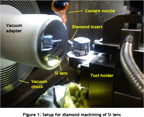
The diamond insert was used to shape a convex lens of 500 mm convexity radius on a 60 mm diameter mono-crystalline silicon piece. The challenge in making this lens lay in its relatively small thickness, which was about 3 mm at the lens edge. Therefore special attention had to be paid to the mounting method and to the force applied. The silicon piece was mounted on a vacuum adapter specially designed for silicon machining. The adapter - an extension of the machine's main vacuum chuck (Figure 1) - was made from ultra-high molecular weight polyethylene characterised by its superior mechanical properties.
In this study, we employed machining conditions that provided ductile mode cutting of silicon on an ultra-high precision machining centre (Nanoform 250 Ultragrind, Precitech). The final convex profile of the silicon lens was shaped at a depth of cut of 5 µm and a feed rate of 2.5 mm/min at a cutting speed of 750 rev/min. These values fall within the range of ductile regime machining conditions tried by other researchers. A flood water-based coolant was used to cool the tool-workpiece interaction zone. In silicon machining, temperature control is absolutely critical: with high localised heating, silicon may suffer from slip dislocations. The diamond tool will also be protected from being overheated because of the low thermal conductivity of the machined silicon.
4. RESULTS AND DISCUSSIONS
Figure 1 shows the final stage of convex lens shaping using the cutting conditions mentioned above. Two inspection steps were performed: on- and off-machine profile measurements. The purpose of this inspection was to compare the actual convex profiles with those of the theoretical ones. Surface roughness of the machined silicon surface was also investigated.
The first profile inspection method is based on using a sensitive gauge constructed from a pneumatic linear variable diffraction transformer (LVDT) with a working range of ±25 µm and a resolution of 12.2 nanometres. The LDVT probe is moved against the machined surface at a low speed, and the changes in the probe axial movements are recorded. Figure 2 shows a graph of the machined surface profile variation of the desired theoretical profile. In this case, the form error (P-V) equals 0.6 µm. The negative sign of the form error of this convex surface indicates that the machined surface is flatter (less steep) than the specified theoretical profile.

The other method used to profile the silicon lens was based on a laser interferometer (from Zygo) to measure the machined surface profile and examine its topography. The wavefront error shown in the interferogram in Figure 3 approaches 22.35 µm (35.322 waves) peak-to-valley, and the surface roughness is 4.5 µm rms. These values indicate that the surface profile exhibited a large error when the silicon lens was removed and measured on an off-process instrument.

The large difference between the two form error values measured by the two methods is explained by the distortion experienced by the lens surface as a result of the vacuum sucking force. The vacuum channels inside the polyethylene vacuum adapter need to be redesigned to realise a more uniform sucking force. The vacuum adapter design should consider providing a sucking force that is just sufficient to hold the machined workpiece. Excessive holding forces will result in a distortion of the part profile after machining.
5. CONCLUSIONS
Ultra-high precision machining using single-point diamond inserts is gaining in popularity over traditional high precision abrasive processes such as grinding and lapping operations when fabrication optical components form mono-crystalline silicon. However, special care should be taken when selecting the machining parameters of silicon diamond turning to facilitate ductile mode cutting. Maintaining a ductile regime during machining of brittle materials such as silicon helps impart the necessary optical properties to the machined surface. However, a point that manufacturing engineers may overlook is the distortion that takes place in the machined surface profile after its removal from the machine chuck. This study revealed the large variation in the form error values measured while the workpiece is mounted on the chuck, and after its removal. The design of the vacuum adapter used to mount the silicon lens needs to consider providing a sucking force just sufficient to hold the machined workpiece.
6. ACKNOWLEDGEMENT
The author would like to acknowledge the NRF's support for the ultra-high precision machine tool, which was sponsored under NEP. The author is also grateful to Mil-Op for their help with the silicon lens interferometry profiling.
REFERENCES
[1] Dumas, D., Fendler, M., Berger, F., Cloix, B., Pornin, C., Baier, N., Druart, G., Primot, J. & le Coarer, E. 2012. Infrared camera based on a curved retina. Optics Letters, 37(4), pp 653-655.
[2] Fang, Z. & Zhao, C.Z. 2012. Recent progress in silicon photonics: A review. ISRN Optics, vol. 2012, Article ID 428690, 27 pages [ Links ]
[3] Suleski, T.J., Davies, M.A. & Dutterer, B.S. 2012. Diamond machining of freeform infrared optics. Intl. Conf. on Optical Fabrication and Testing (OF&T), Optical Society of America, Monterey, California, United States. [ Links ]
[4] Zhong, Z. 2003. Ductile or partial ductile mode machining of brittle materials. The International Journal of Advanced Manufacturing Technology, 21(8), pp 579-585. [ Links ]
[5] Chapman, G. 2004. Ultra-precision machining systems: An enabling technology for perfect surfaces. Moore Nanotechnology Systems. [ Links ]
[6] Zhong, Z. 2002. Surface finish of precision machined advanced materials. Journal of Materials Processing Technology, 122(2), pp 173-178. [ Links ]
[7] Zhong, Z. & Venkatesh, V. 1994. Generation of parabolic and toroidal surfaces on silicon and silicon-based compounds using diamond cup grinding wheels. CIRP Annals-Manufacturing Technology, 43(1), pp 323-326. [ Links ]
[8] Fletcher, D.A., Crozier, K.B., Guarini, K.W., Minne, S.C., Kino, G.S., Quate, C.F. & Goodson, K.E. 2001. Microfabricated silicon solid immersion lens. Journal of Micro-electromechanical Systems, 10(3), pp 450-459. [ Links ]
[9] Alao, A.R. & Konneh, M. 2012. Surface finish prediction models for precision grinding of silicon. The International Journal of Advanced Manufacturing Technology, 58(9-12), pp 949-967. [ Links ]
[10] Brinksmeier, E., MutlugUnes, Y., Klocke, F., Aurich, J., Shore, P. & Ohmori, H. 2010. Ultra-precision grinding. CIRP Annals - Manufacturing Technology, 59(2), pp 652-671. [ Links ]
[11] Leung, T., Lee, W. & Lu, X. 1998. Diamond turning of silicon substrates in ductile-regime Journal of Materials Processing Technology, 73(1), pp 42-48. [ Links ]
[12] Jasinevicius, R.G., dos Santos, F.J., Pizani, P.S., Duduch, J.G. & Porto, A.J.V. 2000. Surface amorphization in diamond turning of silicon crystal investigated by transmission electron microscopy. Journal of Non-Crystalline Solids, 272(2-3), pp 174-178. [ Links ]
[13] Fang, F. & Zhang, G. 2003. An experimental study of edge radius effect on cutting single crystal silicon. The International Journal of Advanced Manufacturing Technology, 22(9), pp 703-707. [ Links ]
[14] Durazo-Cardenas, I., Shore, P., Luo, X., Jacklin, T., Impey, S. & Cox, A. 2007. 3D characterisation of tool wear whilst diamond turning silicon. Wear, 262(3), pp 340-349. [ Links ] ]
[15] Born, D.K. & Goodman, W. 2001. An empirical survey on the influence of machining parameters on tool wear in diamond turning of large single-crystal silicon optics. Precision Engineering, 25(4), pp 247-257. [ Links ]

