


Serviços Personalizados
Artigo
 Inglês (pdf)
 Artigo em XML
 Referências do artigo
Indicadores

Links relacionados
-
 Citado por Google
 -
 Similares em Google
Compartilhar

 Permalink
SAIEE Africa Research Journal
versão On-line ISSN 1991-1696
versão impressa ISSN 0038-2221
SAIEE ARJ vol.114 no.4 Observatory, Johannesburg Dez. 2023
GaN HEMT Power Amplifier Design for 2.45 GHz Wireless Applications
Paula Akossiwa AtchikeI; Jamal ZbitouII; Ahmed El OualkadiI; Pascal DherbécourtIII
ILaboratory of Innovative System Engineering, ENSA Tetouan, Abdelmalek Essaadi University, Avenue Palestine B.P 2222, M'hannech II-Tetouan, Morocco. (E-mail: aeloualkadi@uae.ac.ma, akossiwapaula.atchike@etu.uae.ac.ma)
IILaboratory of Information and Communication Technologies, ENSA Tangier, Abdelmalek Essaadi University, Tetouan, 93000, Morocco. (E-mail: j.zbitou@uae.ac.ma)
IIIUniv Rouen Normandie, INSA Rouen Normandie, CNRS, Normandie Univ, GPM UMR 6634, F-76000 Rouen, France. (E-mail: pascal.dherbecourt@univ-rouen.fr)
ABSTRACT
Electronic devices with high performances like Power Amplifiers (PA) are very important for Wireless communications. This paper proposes a design of a class AB power amplifier operating at 2.45 GHz, in the S-band frequency. The Cree's CG2H40045F GaN HEMT (High Electron Mobility Transistor) is used for this design. The Gallium Nitride (GaN) technology has been chosen in light of its advantageous properties such as high breakdown voltage, high band gap, as well as high thermal conditions. The paper investigates the different design trade-offs for finding a good balance between various key parameters of the PA (linearity, efficiency, and gain). A design approach has been proposed and the microstrip lines based on the Smith Chart tool available in ADS software have been used for the matching process. The class AB was selected to reach a good agreement between linearity and efficiency, provided by this class. After various process applications from DC characterization to simulations, the proposed design achieves a power added efficiency more than 50% at power saturation with a gain of 15 dB in schematic simulation. The layout dimensions are 55.5 x 64.45 mm2 on PCB technology.
Index Terms: Class AB, efficiency, gain, GaN, High Frequency, matching, PA.
I. Introduction
Wireless communications evolution involves high-performing Radiofrequency (RF) devices design. Among them, we have Power Amplifiers (PA) that are essential to the transmission chain. PAs boost up signal in the RF transmitter, which is radiated by the antenna and caught by the receiver[1]. Various past works have studied this device's design using different transistor technologies and approach for miscellaneous applications. Several transistor technologies can be used for RF amplifiers, but GaN HEMT technology is a good choice due to its important characteristics which makes it very interesting for RF applications [2-3-4]. Indeed, this technology is characterized as: wide bandgap (3.4 eV) while Silicon bandgap is 1.12 eV; thus GaN tends to be used instead of Silicon[4] to improve power conversion and energy efficiency. A wide energy bandgap allows the device to support high electric fields. Then GaN has a high breakdown voltage (3.3 MV/cm), which involves large drain voltage operation. A high thermal conductivity (1.7 W/cm.K), also characterizes the GaN technology. A high thermal conductivity results in appropriate temperature working. Furthermore, this technology has the ability to make heterojunctions traduced by high electrons mobility (1000 cm2/V.s). The GaN technology was chosen for these characteristics in spite of several others like CMOS technology used in [3]. It was proposed in [3] a software routine in order to design a PA on class E or F. However, the proposed design uses only lumped elements and shows a decrease in performances like output power. The design of PA with GaN technology can be completed with different approaches. For instance, envelope tracking (which is the power supply adjustment with the aim to overlap it with signal envelope), was used in [4]. This technique enhance the Power Added Efficiency (PAE), and the simulated value is 55% at 2.45 GHz, while the used GaN transistor could give a value of PAE over 65%. Another works on PA design were made with GaN transistor: such as PA design for radar in [5], using harmonic load network at 2.4 GHz; but also PA design using harmonic tuning at 2.45 GHz ISM frequency in [6]. In these works, good performances were reached but reflection coefficients values don't exceed -15 dB in schematic simulations. Besides, the harmonic tuning used by the previous works, there are other methods in PA design like the internal matching impedance method [7] and, the load pull method [8]. In these quoted works, different approaches were used to design a PA but either the efficiency, or the gain, or the power saturation, or the reflection coefficients were not great as intended. In fact, the challenges in designing a PA are finding the appropriate way to define impedances in the circuit, the design of functional matching networks and in the same time, finding the trade-off between PA parameters. This paper investigates on simple process for PA design with a GaN HEMT transistor operating at 2.45 GHz frequency using ADS software. The bilateral approach was applied in this design with microstrip lines for matching issues based on smith chart. The designed PA achieves a good trade-off between the gain, the efficiency, and the linearity even in electromagnetic simulation (EM). A non-linear model of the chosen transistor was used. In this design, the class AB was preferred owing to good balance between class A with a good linearity and class B with a good efficiency from 50 to 78% [9]. The working frequency f = 2.45 GHz was chosen for Wi-Fi technology and 802.11n standards [10-11]. This paper is organized as follows. Section II presents the proposed PA design, including the bias, the matching networks, and the layout. The results are presented in section Ill, and the conclusion is given in section IV.
II. Proposed Power Amplifier Design
A. PA structure
The core of the PA is the transistor and in this paper, the CG2H40045F GaN HEMT transistor has been chosen for its frequency band working from 2 to 4 GHz; a band frequency suitable for wireless communications, especially for 2.45 GHz applications [12]. This transistor can produce 14 dB small signal gain at 4 GHz and 18 dB at 2 GHz and is also class AB operational, therefore the expected efficiency will be high (60% according to the datasheet). A power amplifier is a circuit resulting from joined blocks which are the bias and matching networks. As shown in Fig. 1, these blocks are available at both the PA circuit input and output.
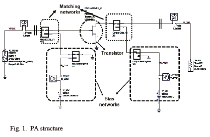
Bias networks are useful to fix an operating point and to decouple RF and DC signals. The matching circuits minimize power reflection to ensure a maximum power transmission. The design of PA is resumed on designing these blocks, for this reason, a design flow is needed.
B. Design flow
To achieve the design of PA, a design flow has been proposed to make different steps clear. The Fig. 2 shows the proposed PA design flow. The first step is a DC characterization of the chosen transistor (CG2H40045F). This initial step is essential for fixing the transistor operating point. Then the stability and the matching issues are considered. A good matching means that S parameter reflection coefficients are low and the performances like output power, gain and efficiency are closed to predicted performances in the transistor datasheet. Since the circuit was built with the represented components available in the used software, a layout conception and a post layout simulations (also called EM co-simulation), are important finalizing steps in a PA design before moving to a practical realization of the circuit.
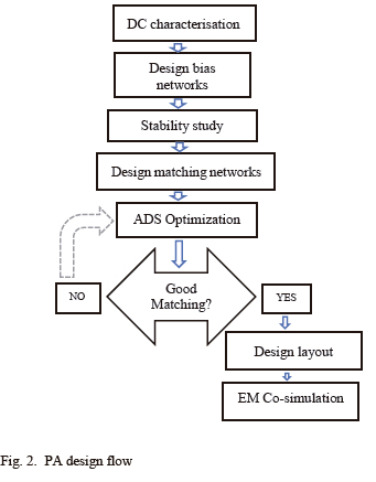
To achieve all tasks, a professional designing software ADS (Advanced Design System) has been used. This software offers possibility to simulate numerous microwave circuits or complex systems [13]. Thanks to this software multifunction, the opportunity is also given to designer to optimize his results with available methods [14]. This is the ADS optimization that we include in the design flow.
C. DC characterization
This stage is important in the task of fixing the DC bias quiescent point which depends on the chosen class of the PA. Fig. 3 shows the transistor drain current variations depending on drain voltage for constants gate voltage values. In this case of class AB, we locate this point with load line help [15]. This line results from two points: the first point is located at the limit of the linear zone and the second point at the limit of the saturation zone as shown in Fig. 3.
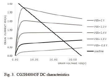
Referring to the transistor datasheet[12], two possibilities for bias point are available for this transistor. The quiescent bias point reserved for our transistor is located in class AB, on load line at VDs0 = 28 V for drain supply; VGs0 = -2.625 V for gate supply and IDS0 = 0.8 A for drain current. To set this point, it is important to build the bias networks.
D. Bias network
As already defined, the bias network is useful to provide DC supply according to the bias point and also to decouple both RF and DC signals. The structure of the proposed bias network is made with a quarter wave line which behaves like an RF choke. By considering a transmission line represented in Fig. 4, the input impedance can be calculated according to the transmission lines theory[16].
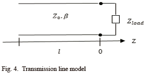
The transmission line impedance equation is given by:
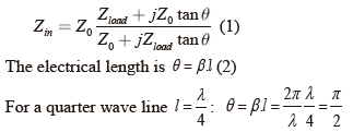
Where β is the propagation constant, l the line length and λ the wavelength.
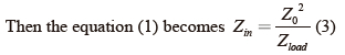
Equation (3) is the expression of the input impedance of a quarter wave transmission line. For a high value of Z0 this line can similarly behave like an open circuit. Thus to get the RF choke behavior, the chosen bias structure is made with a high impedance quarter wave line (Z0 = 100 Ω). The RF choke role is to block the RF part around the operating frequency and therefore protect the bias voltage from RF signal [17]. If ever a RF part has managed to pass, it will find a capacitor with a value of 100 pF, which has the role of routing the leaked RF signal to the ground; this is to ensure a perfect decoupling. The final network is shown in Fig. 5.
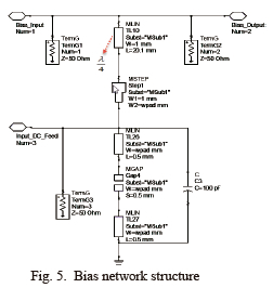
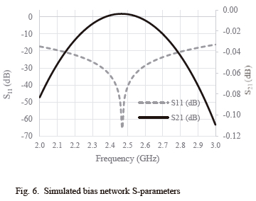
As shown in Fig. 6, the values of the S-parameters at f = 2.45 GHz frequency are: S21 = -0.004 dB for transmission coefficient (value close to zero) and S11 = -50.77 dB, for the reflexion (low value) coefficient, then the isolation is good.
E. Small signal stability
The stability notion is very important to remove any oscillation risk and should be carefully checked during the design process. PA is unconditionally stable if Rollet factor K >1 and|Δ|< 1 [1]. These factors are calculated with the S-parameters of the polarized transistor, before the matching process.
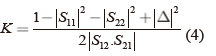
Where Δ = S11.S22 - Sl2.S21
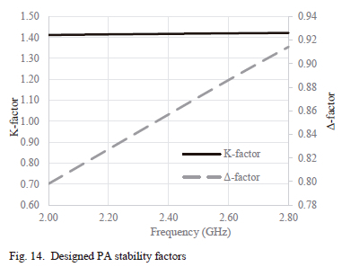
The results of the simulated value of these two factors are shown in Fig.7.
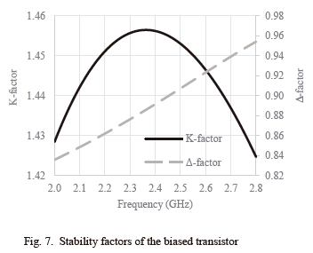
At the operating frequency f = 2.45 GHz, K = 1.455 and |Δ| = 0.899. Since we have K > 1 and|Δ| < 1, then the transistor is unconditionally stable at the operating frequency.
F. Matching networks
In the literature, there are various gain equations defined in the power amplifier design like GT (transducer power gain),
which is the ratio of power delivered to the load to the power available from the source. There is also Gp (operating power gain) which is the ratio of power dissipated in the load to the power at the network input, and Ga (available power gain) which is the ratio of the power available from the network to the power available from the source. [18]
The transistor's unconditional stability allows for a bilateral approach to be used in PA design, by considering that the transmission coefficient from device input to output called S12 parameter, was not neglected S12 ≠ 0 [18]. This approach means that when the input and output of circuit are both matched, the gain is maximized. Then the three defined gains are equal to:
Where Gmax can be calculated by:
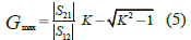
By considering the transistor S-parameters and stability simulations results at f = 2.45 GHz frequency:

The calculated value of Gmax is 16.75 dB. This is an indicator to check the gain performance of the PA.
When bilateral approach is used in the matching process, this involves simultaneous matching networks at both the input and output of the circuit. Then, impedances definition in the circuit are necessary. In order to maximize the gain of the PA, the Ga gain can be used in the impedance searching in the circuit. Actually, for a given value of Ga, a constant available power gain circle is plotted with integrated Ga circle tracer in ADS. Ga expression is given by:
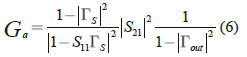
Where Γs is the reflection coefficient at the source of the circuit and Γout, is the reflection coefficient at output of transistor. In this study, we want to reach a gain value of 16 dB, according to Gmax value. Then the circle of Ga = 16 dB is plotted and it is known that all Γs on this circle produce the given Ga [1]; then, the source impedance can be defined.
So according to Fig. 8, we get our input impedance Zs =3.762 - J6.729.
For the output impedance we simply use the value derived by the load reflection coefficient. By plotting S parameters, the corresponding value at output is Zl = 9.325 + j5.557.
There are several matching methods [14] and in this case we use bilateral approach with transmission lines impedance transforming abilities [14].
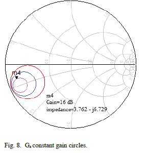
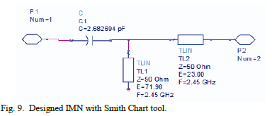
Then, with these found impedance values, we design both the Input Matching Network (IMN) and Output Matching Network (OMN) by using Smith chart. We incorporate capacitances which act like DC blocks as we already mentioned. The DC blocks were directly integrated during the matching design to avoid disturbing the process. In the previous section, it has been already mentioned that, the best place for the block capacitance is just after the RF signal generator at the input and just before the load at the output. This is to protect the RF signal generator at the input and the output against the DC signal from the transistor bias source [18]. Matching networks are also made with open shunt stubs and series stubs. The designed IMN and OMN by using Smith Chart are shown in Fig. 9 and Fig. 10 respectively.
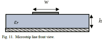
After using Smith Chart tool for matching networks design, the result is ideal transmission lines characterized by electrical length θ and characteristic impedance Z0. Then, linecalc tool is used to convert the ideal lines into microstrip lines. This tool use the electrical characteristics of the ideal transmission line known as the electrical length 9 and characteristic impedance Z0 to make the conversion to physical characteristics of the microstrip line which are the width w and the length l.
For a given Z0 and a dielectric constant εr, the ratio  is:
is:
As long as the height of substrate h is given, the value of the microstrip line width w can be calculated with the previous expressions[19].
The second physical characteristic of the microstrip line is the length l, which can be calculated by:
Where, θ is the electrical length, c is the velocity of light in a vacuum, f the frequency and εe is the effective dielectric constant which can be considered as the dielectric constant of a homogeneous medium that equivalently takes the place of air and dielectric regions of the microstrip line.
The "linecalc" tool available on ADS gives the correspondent microstrip line characteristics like width and length. The used substrate is RT/duroid6002, characterized by the height h = 0.508 mm and εr = 2.94 [20].
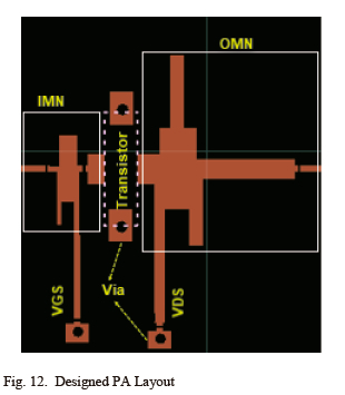
G. Layout and cosimulation circuit
The proposed PA layout is shown in Fig. 12. The PA is implemented on Rogers RT/duroid 6002 substrate and based on CG2H40045F active device. The layout shows both the input and output matching networks, the biasing networks and both the gate and drain paths all, are designed using microstrip transmission lines. According to datasheet transistor the dimensions of the GaN HEMT transistor are: 6 on 15 mm. The layout sizes are 55.5 mm on 64.45 mm.
The Fig. 13 shows the model generated from the designed layout which can be used for EM co-simulation. It is called co-simulation because in the same schematic, layout electromagnetic model and the others circuit elements that cannot be represented in the layout, like power generators, are all simulated together.
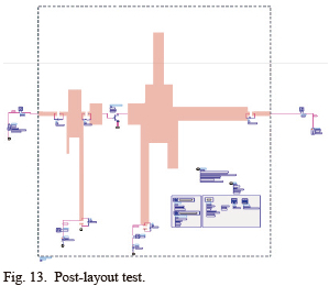
This kind of simulation is indeed important for considering electromagnetic phenomena occurring in the circuit [21], especially in microstrip lines use.
III. Simulation Results
The performances of the simulated PA are presented in this section. First, the stability factors simulations are very important for checking the designed PA stability.
The performances are evaluated in terms of output power, gain, and efficiency. Before moving forward, the checking of s-parameters is also important.
As shown in Fig. 14 the Rollet factor at the operating frequency f = 2.45 GHz is: K = 1.435 and |Δ| = 0.835. K > 1 and|Δ| < 1, then we conclude that the designed PA is stable at the operating frequency; oscillations risks are removed.
The obtained PA at the end of a design must present the low values of reflection coefficients. In other words S11 and S22 must be low as possible. This is a sign of good matching. The transmission coefficient S21 gives an overview of the gain. The S12 factor represents the feedback from the output to the input. This factor must necessary be small for the reason that it is the most representative factor of isolation.
Fig. 15 shows the S-parameters values obtained at f = 2.45 GHz operating frequency. It can be observed that the designed PA shows a good matching since the obtained parameters S11 and S22, are equal to -47.799 dB and -46.094 dB in schematic simulation, respectively. Transmission coefficients are also a part of S-parameters: S12 and S21, are equal to -24.707 dB and 16.871 dB respectively.
The variation of the simulated output power versus input power at f = 2.45 GHz frequency, both before and after co-simulation is shown in Fig. 16. These plots show the PA power limitations and the compression point. As observed, the compression point is at P1dBm = 27 dBm and the power saturation is Poutmax = 46.9 dBm for schematic simulation. However, for EM simulation, the compression point at the input power is P1dBm = 28 dBm and the power saturation is Poutmax = 47.5 dBm for EM simulation. The maximum value of output power extracted from the datasheet is 46.5 dBm.
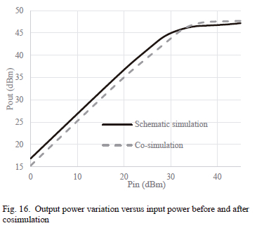
The compression point P1dBm is the point at which the output power value is 1dB lower than the power value in the ideal linear response.
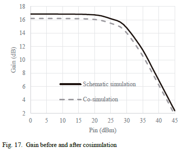
The most important PA performance is the power gain which is the ratio between output power and input power [18]. The Fig. 17 shows the variation of the simulated gain versus input power at 2.45 GHz frequency before and after co-simulation. At the compression power, the gain is equal to 15.85 dB for schematic simulation. However, after EM co-simulation, the gain is equal to 14.018 dB. Knowing that this transistor can produce a gain from 14 dB to 18 dB[12], and the expected value is Gmax = 16.75 dB; the obtained result is still acceptable.
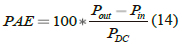
The Power-Added Efficiency (PAE) is a metric for rating the efficiency of a power amplifier. This efficiency takes account the effects of the input power. The input power, output power and the DC power are used to as given in equation (14):
The obtained PAE value is 65.9% at power saturation before co-simulation and equals 59.2% after, according to Fig. 18. In the transistor datasheet [12], 60% of efficiency value is expected.
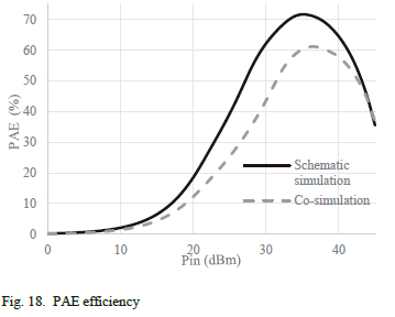
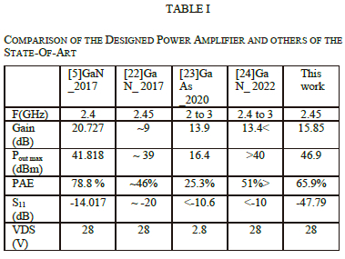
Table I summarized the obtained results of the proposed design compared to similar works in the state-of-the-art. By comparing the obtained results of this work to others in the literature, the proposed GaN HEMT PA exhibits a good output power with a good PAE, a high gain and an excellent impedance matching with a simple approach. These reasons make the designed PA suitable for wireless communication applications operating at 2.45 GHz frequency.
IV. Conclusion
A power amplifier designed at 2.45 GHz with CG2H40045F GaN HEMT transistor in class AB is proposed in this paper. This technology is suitable for high frequency applications and power amplifier performance. To achieve the goal, this conception starts with DC characterization, followed by stability considerations and then matching issues. For matching, the bilateral approach is used, Smith Chart implemented in ADS has been used and we end up with microstrip matching networks. After post layout tests of the achieved PA, we noticed Poutmax equals to 46.9 dBm; a gain equals to 15.85 dB and more than 50% PAE efficiency. These results make this design suitable for wifi application. The next step will be to carry out a real prototype of this amplifier.
Acknowledgment
We want to thank the Professor Ahmed Errkik, Hassan Premier University, Settat, Morocco, and the Professor Yassine Bouslimani, University of Moncton, Canada, for their collaboration on this project.
References
[1] David M. Pozar, "Introduction to microwave systems," Microwave Engineering, John Wiley & Sons Second edition. 1998, pp. 662-671.
[2] M. Golio, RF and microwave semiconductor device handbook, Boca Raton London New York Washington, D.C., 2003.
[3] M. Bozanic and S. Sinha, "Design approach to CMOS based Class-E and Class-F power amplifiers," SOUTH AFRICAN Inst. Electr. Eng., vol. 100, no. 3, pp. 79-86, 2009. [ Links ]
[4] P. Suebsombut, O. Koch, and S. Chalermwisutkul, "Development of a GaN HEMT class-ab power amplifier for an envelope tracking system at 2.45 GHz," in ECTI-CON 2010, pp. 561-565.
[5] K. S. Pradeep, C. C. Chowdhary, P. Poornima, and K. Ramya, "Design and implementation of class-F GaN HEMT power amplifier for S-band radar," ICEECCOT 2017, vol. 2018-Janua, pp. 103-109, 2018, doi: 10.1109/ICEECCOT.2017.8284648.
[6] M. Góralczyk and W. Wojtasiak, "ISM 2.45 GHz band high-efficient 15 W GaN HEMT power amplifier: Design validation," in IJMWT Sep. 2019, vol. 11, no. 7, pp. 546-553, doi: 10.1017/S1759078719000631. [ Links ]
[7] F. Li and S. C. Zhong, "An S-band Wideband High power GaN HEMT Power Amplifier," CSRSWTC 2020 - Proc., Dec. 2020, doi: 10.1109/CSRSWTC50769.2020.9372600.
[8] Y. Ban and J. Liu, "A compact power amplifier based on a 5 W GaN HEMT in S-band application," 2020 IEEE APCAP 2020 - Proc., Aug. 2020, doi: 10.1109/APCAP50217.2020.9246158.
[9] S. C. Cripps, , "Class AB amplifiers," Advanced Techniques in RF Power Amplifier Design, Artech House Boston, 2002, pp. 1-32.
[10] K. Fazel and S. Kaiser, Multi-carrier and spread spectrum systems : from OFDM and MC-CDMA to LTE and WiMAX, Second edition. United Kingdom, 2008.
[11] M. H. Chen, M. C. Huang, Y. C. Ting, H. H. Chen, and T. L. Li, "High-frequency wireless communications system: 2.45 GHz front-end circuit and system integration," IEEE Trans. Educ., vol. 53, no. 4, pp. 631-637, Nov. 2010, doi: 10.1109/TE.2009.2038897. [ Links ]
[12] Cree Wolfspeed, "Datasheet CG2H40045," Large Signal Model. Available ADS MWO, 2021.
[13] Agilent Technologies, "Agilent EEsof EDA Advanced Design System Circuit Design Cookbook2.0," USA, 2012.
[14] R. Gilmore, and L. Besser, "CAE/CAD of linear RF/MW circuits," Practical RF Circuit Design for Modern Wireless Systems: Passive Circuits and Systems, Artech House Boston., vol. I. Artech Print on Demand, 2003, pp. 277-298.
[15] S. C. Cripps, "Class AB PAs at GHz Frequencies," RF Power Amplifiers for Wireless Communications, Second Edition. 2006, pp. 67 -74.
[16] B. C. Wadell, Transmission line design handbook. Artech House, 1991.
[17] L. Besser and R. Gilmore, "Linear RF amplifier design," Practical RF Circuit Design for Modern Wireless Systems: Active Circuits and Systems, vol. II. 2003, pp. 59-70. [ Links ]
[18] David M. Pozar, "Design of microwave amplifier and oscillators," Microwave Engineering, John Wiley & Sons Second edition. 1998, pp. 600-632.
[19] David M. Pozar, "Transmission lines and Waveguides," Microwave Engineering, 4th Edition. University of Massachusetts at Amherst, John Wiley & Sons, 2012, pp. 144-153.
[20] R. Corporation, "RT/duroid 6002 Laminates Data Sheet," pp. 1-2.
[21] D. G. Swanson and W. J. R. Hoefer, Microwave Circuit Modeling Using Electromagnetic Field Simulation, London, 2003.
[22] D. Banerjee and M. Hashmi, "Design of GaN HEMT Broadband Power Amplifiers by Deepayan Banerjee," New Delhi , Mar. 17AD.
[23] L. Mohammed, Z. Lahbib, and S. Adil, "Approach for the Design of a Broadband Microwave Power Amplifier in Microstrip Technology for Mobile Communications Systems," Indones. J. Electr. Eng. Informatics, vol. 8, no. 2, pp. 289-297, 2020, doi: 10.11591/ijeei.v8i2.1701. [ Links ]
[24] M. Soruri, S. M. Razavi, and M. Forouzanfar, "Design and Optimizing of a GaN HEMT Power Amplifier Based on the Inclined Planes System Optimization Algorithm for Wireless Applications," Iran. J. Electr. Electron. Eng., vol. 18, no. 3, p. 2369, 2022, doi: 10.22068/IJEEE.18.3.2369. [ Links ]
This work is supported by Agence Universitaire de la Francophonie and Ministère de l'Enseignement Supérieur, de la Recherche Scientifique et de l'Innovation, Morocco. Under Code ANC2 DRM-6871.

Paula ATCHIKE was born in Benin, in January 1998. She received her Master degree in Electronic and telecommunications at ENSA of Abdelmalek Esaadi University, Tangier, Morocco, in October 2021. Following this she start her PhD studies at the same structure since 2021. Her research studies are relative to power amplifier design and GaN technology reliability.

Jamal Zbitou was born in Fes, Morocco, in June 1976. He received a Ph.D. degree in electronics from Polytech of Nantes, the University of Nantes, France, in 2005. Currently He is a Full Professor in Electronics and Telecommunications, LABTIC, ENSA of Tangier Abdelmalek Essaadi University. He is involved in the design of the hybrid, monolithic, active, and passive microwave electronic.

Ahmed El Oualkadi received Ph.D. degree in electronics from the University of Poitiers, France, in 2004. In 2005, he joined the Microelectronics Laboratory at the University Catholic of Louvain, Belgium, where he worked on the analog & mixed design of low power high temperature circuits, for wireless communication. Currently, he is the Deputy Director of Scientific Research and Cooperation National school of applied sciences of Tetouan (ENSATe) in the Abdelmalek Essaadi University, Morocco. His main research interest is the analog IC, mixed-signal & RFIC design for wireless communication, embedded system applications & information technology. He is a member of EuMA and an IEEE volunteer member associated to the Circuits & Systems Society where he is a reviewer of IEEE. He is a member of the scientific and technical committee of WCECS & WASET, a member of the editorial board of Journal of Multimedia Processing and Technologies & during 2007-2011, he was an editorial board member of Recent Patents on Electrical Engineering Journal edited by Bentham Science Publishers.

Pascal Dherbécourt is head of the electrical engineering bachelor of institute of technology in University of Rouen - Normandie, France. He received a diploma degree and a Ph.D in physics and electronics in 2002. Over the period from 1999 to 2008, he worked in the field of optical fibers telecommunications. In 2008, he joined the GPM (Groupe de Physique des Matériaux, UMR CNRS 6634) and became co-founder of ErDefi team (research team in reliability and failure analysis of electronic components, become Er2MD in 2021). His main research interest is now reliability and failure analysis of high-power transistors for telecommunication and radar applications and for power convertors. He participates in numerous research projects in collaboration with major companies. Since 2017 he participates in the development of training radars and microwave teaching programs for aeronautics and telecommunication business.

