


Services on Demand
Article
 English (pdf)
 Article in xml format
 Article references
Indicators

Related links
-
 Cited by Google
 -
 Similars in Google
Share

 Permalink
SAIEE Africa Research Journal
On-line version ISSN 1991-1696
Print version ISSN 0038-2221
SAIEE ARJ vol.111 n.4 Observatory, Johannesburg Dec. 2020
REGULAR PAPER
A Novel Low Line Regulation CMOS Voltage Reference Without BJTs and Resistors
Changqing Zhang; Xia Wu; Wanling Deng; Junkai Huang
Department of Electronic Engineering, Jinan University, Guangzhou 510630, China. Corresponding author is Junkai Huang (e-mail: hjk196310@126.com), Changqing Zhang (e-mail: 463971191@qq.com), Xia Wu (e-mail: 726558441@qq.com), Wanling Deng (e-mail: dwanl@126.com)
ABSTRACT
A novel CMOS-only low line regulation voltage reference is presented in this paper. An output subcircuit composed of MOSFETs operating in the subthreshold region and saturation region is utilized to eliminate the temperature dependence of mobility and oxide capacitance, and produces a temperature-insensitive voltage reference. No bipolar junction transistors (BJTs) or resistors are used which can decrease the area greatly. By using most of the transistors operating in the subthreshold region, the power dissipation and the supply voltage are reduced. The proposed voltage reference is designed in the standard 0.18 μm CMOS process. The simulation results show that the output voltage is 958.971 mV at TT process corners, a temperature coefficient of 18.6096 ppm/°C range from -20 °C to 110 °C is achieved, the line regulator (LR) of the proposed circuit is 0.037 mV/V from 1.5 V to 2.5 V supply voltage, and the power supply rejection ratio (PSRR) is -75.77 dB at 100 Hz. The active area of the presented voltage reference is 0.0038 mm2.
Keywords: voltage reference, resistors, temperature coefficient,LR, PSRR.
I. INTRODUCTION
Voltage reference (VR) circuit is an indispensable unit module in integrated circuit, and is used to provide a stable direct current (DC) reference, which is hardly affected by temperature drift, process variation and voltage fluctuation. Therefore, high precision references with low sensitivity to temperature, process, and supply voltage variations play an important role in many applications, such as analog-to-digital converters (ADC), digital-to-analog converters (DAC), phase-locked loops (PLL), oscillators (OSC), linear voltage regulators, memory and power management chips etc. [1]-[5].
Traditional bandgap reference (BGR) [6]-[8] is implemented by adding two voltages or currents with opposite temperature characteristics, thus producing a voltage independent of absolute temperature. In this method, the base-emitter voltage (VBE) of bipolar junction transistors (BJTs) is usually used to generate a negative temperature coefficient (TC) voltage, and the positive TC voltage is generated by using resistors and thermal voltage (VT). As VEB is not a linear function of temperature, the voltage with low TC cannot be achieved without first or high order temperature compensation [9]. In order to solve this problem, a large number of compensation circuits are proposed, such as logarithmic-curvature compensation circuit, piecewise liner compensation circuits, etc.
[10]-[11]. Although this method can compensate the TC of these circuit well, the use of these BJTs and resistors will occupy a large area, and will also require a high supply voltage and a complex compensation circuit.
Based on such problems, the CMOS VRs without BJTs have been proposed in [12]-[13]. In [12], the mutual temperature compensation principle of the threshold voltage of NMOS and PMOS transistors is utilized to obtain temperature-insensitive VR. In [13], the body bias compensation is employed, and its TC and LR are 48 ppm/°C and 3.4 mV/V respectively. In addition, the voltage reference composed of MOSFETs-only is also proposed in [14]-[15]. In [14], a curvature-compensation method is used to cancel logarithmic temperature dependence of mobility in the circuit, where the TC can be reduced to 7 ppm/°C and the PSRR achieves -43 dB. In [15], the design of VR uses the principle of the theramal compensation of a series composite NMOSTs to obtain reference output voltage whose LR can reach 2.217 mV/V and the TC can be reduced to 19.302 ppm/°C. All of these studies can compensate the TC well, and the BJT or resistor is not introduced in the circuit. However, some new issues such as high LR and low PSRR may follow.
In this paper, we propose a novel CMOS VR. It should be noted that there are no BJTs or resistors used in the circuit. By the use of the transistors operating in the subthreshold region and a MOS resistor operating in the triode region, the area of the proposed VR can be greatly decreased. Since the current source subcircuit uses the feedback technique, the amplifier is omitted, the line regulator (LR) is improved, and the power supply rejection ratio (PSRR) achieves -75.77 dB. The temperature compensation is obtained by using the output subcircuit which is composed of MOSFETs operating in the subthreshold region and saturation region, and it adjusts the output voltage. The proposed design achieves less temperature sensitivity and a smaller line sensitivity. Therefore, the voltage reference can be used in Comparators, A/D and D/A converters, DC-DC converters, and PLLs and so on. The voltage reference can be applied to mini-computers, wearable electronic devices, wireless sensors, smart phones etc. The working principle of this circuit, simulation verification, and other details will be discussed in the following sections.
II. PRINCIPLE AND ARCHITECTURE OF PROPOSED VR
The principle of our voltage reference is illustrated in Fig. 1.

This work was supported by the Guangdong Natural Science Foundation under Grant 2020A1515010567.
The circuit consists of start-up circuit, current source subcircuit, and output subcircuit. The current source subcircuit uses a MOS resistor MR1 operating in strong-inversion and deep-triode regions instead of ordinary resistors. It generates the current Iref. The output subcircuit accepts current Iref though PMOS current mirrors operating in the saturation region and produces an output voltage (i.e., reference voltage), Vref. All the MOSFETs except for MR1, MN4, MN5, MN7, and PMOS current mirror are operated in the subthreshold region. The circuit generates two voltages with a negative temperature coefficient (TC) and a positive TC. Then, it adds them together to produce a constant voltage with a zero TC. The operation and design considerations of each block will be discussed in the following sections.
A. Principle of temperature compensation
The current source subcircuit is illustrated in the middle of Fig. 1. All the MOSFETs except for MP5 - MP7 and MR1 are operated in the subthreshold region. The subthreshold drain current Id of a MOSFET is a function of temperature. If the source-drain voltage VDSsatisfices VDS> 4VT[16], it can be written as

where μx is the temperature-dependent carrier mobility as μ(T) = μ0(T/T0)-m [17], m is a constant about 1.5-2, COXis the oxide capacitance per unit area, S is the subthreshold slope factor, K is the transistor aspect ratio as K= W/L, VTis the thermal voltage and VT=KBT/q, KBis the Boltzmann constant, q is the elementary charge, VDSis the drain-source voltage, VTHis the threshold voltage, and VGSis the gate-source voltage.
The structure of negative feedback loop introduced by MP3, MN8, MP5, MP7, MN2 and MN1 is shown in the current
source subcircuit of Fig. 1. Due to the negative feedback, the voltage of node c is stable. Therefore gate-source voltage VSG(MP1)in MP1 is equal to the sum of gate-source voltage VSG(MP2) in MP2 and drain-source voltage VDS(MR1)in MR1, i.e.,

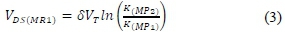
here, VSG(MP1)and VSG(MP2)are the gate-source voltages of MP1 and MP2, respectively. VDS(MR1)is the drain-source voltage of MR1. All symbols in subscript brackets correspond to transistors. Substituting (2) into (3), we can get the expression, i.e.,
MOS resistor RMR1 are operated in a strong-inversion, deep-triode region, so its resistance RMR1 is given by

Using (2), (3), and (4), the bias current Iref of MP7 can be derived as

In the output subcircuit, all the MOSFETs except for MN3 and MN6 are operated in the saturation region, and MN3 and MN6 are operated in the subthreshold region. For Iref, the gate-source voltages of transistors MN3 to MN7 form a closed loop, and the currents of MN4, MN5 are respectively denoted as 3AIref and 2AIref, where A = KMP8/KMP7. We find that output voltage Vref of the circuit is given by

The I-V characteristic of an n-MOSFET operating in the saturation region can be approximated by [18]

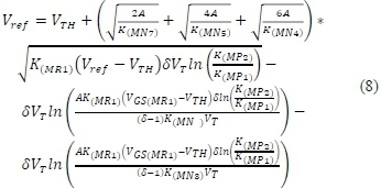
where X is the channel length modulation coefficient. This designed circuit use long channel device to suppress the effect of channel length modulation. Substituting (1), (5) and (7) into (6), the Vrefcan be rewritten as
where we assumed that the mismatch between the threshold voltages of the transistors can be ignored. Besides, the temperature dependence of the threshold voltage can be given by

where Vtho is the threshold voltage at 0 K, a is TC of Vth[11]. Substituting (9) into (8), the Vref can be given by

In this designed circuit, when the TC has the smallest value, the relation of Vref- Vtho« KT can be developed [19]. As a result, Vrefcan be rewritten as
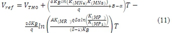
where

According to (11), a zero TC voltage can be obtained by choosing a proper k(i)on condition that
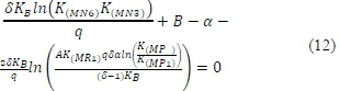
Therefore, we can get a high-precision voltage reference based on the above temperature compensation principle.
B. Negative feedback analysis
The channel length modulation effect causes variation of the output voltage and the bias current when the supply voltage varies [20]. The LR performance is a DC parameter, which
represents the variation of output voltage caused by the input supply change. On the other hand, PSRR is defined as PSRR = 20lg(∆Vref/∆VDD) It is not only the complement of supply gain but it also includes the entire frequency spectrum. Therefore, A voltage reference that is insensitive to the supply voltage is very important. In Fig. 1, a negative feedback loop composed of MP3, MN8, MP5, MP7, MN2 and MN1 is introduced to improve the performances of PSRR and LR. If the voltage Vd of the node d rises with the supply voltage variation, Ve would drop, and Vc would rise. Since the gain of the negative feedback loop is greater than the positive feedback loop gain introduced by MN1, MN8, MP5 and MP6, Vd would fall at last. In addition, MP1-MP3 working in the subthreshold region are diode connected, and their Vds voltages are much larger than 4Vt, so they are almost constant for the small variation of bias current. Fig. 2 shows the small signal model of the current source subcircuit at low frequencies.


Herein, gmni and gmpi represent the transconductances of MNi and MPi, respectively. The output resistances of MPi and MNi are marked as topi and roni, respectively. Vdd is the supply voltage. Through (13)-(17), we can get the expression. i.e.,

where

Fig. 3 shows the small signal model of the output subcircuit. Similarly, we can get the following expressions:

Through (19)-(23), we can get

where

Using (18) and (24), Vref/VDDcan be written as

where

From (25), we can deduce that the sensitivity of Vref to VDDis proportional to gmp3/gmp5, gmr1, and gmp8. By adjusting the transistor aspect ratio of MP9, MN5, MN6, etc., the LR can be further improved. Therefore, the VR independent of VDD can be obtained by reasonably adjusting the aspect ratio of MPi and MNi.
III. SIMULATION RESULTS AND DISCUSSION
In order to verify the performance of the proposed VR, a series of simulation results have been implemented under the TSMC 0.18 um CMOS process.
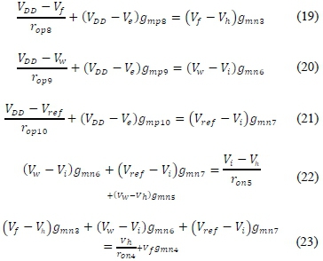
Fig. 4 shows the simulation results of the output voltage Vref versus temperature at various supply voltages. When the supply voltage varies from 1.5 V to 2.5 V, the minimum and maximum values of Vrefin the range from -20 to 110 °C are 958.971 mV and 959.008 mV, respectively. Under four different supplied voltages, the average value of TC is about 18.6893 ppm/°C, and the maximum deviation of the temperature coefficient is 0.1598 ppm/°C.
The Vrefof the proposed circuit versus temperature at different process corners is shown in Fig. 5, where the best case occurs at the SS process corner whose TC is 18.2362 ppm/°C, while the worst case occurs at the FS process corner whose TC is 23.3690 ppm/°C, and the difference between them is 5.1328 ppm/°C. This simulation result is consistent with the derivations of (10) to (12). Therefore, under different supply voltages and process corners, the output voltage Vrefhas a stable TC.

Fig. 6 shows that Vrefvaries with Vddat different temperatures. Obviously, curves with different temperatures have similar trends and due to the proposed circuit structure, the circuit begins to output the stable Vref after Vdd= 1.5 V.

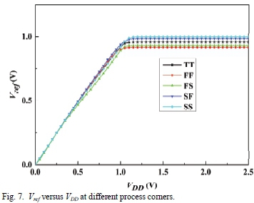
Fig. 7 shows that Vref varies with Vdd at different process corners when the supply voltage is 1.5 V. It is clearly that the output voltage is almost constant when the supply voltage is greater than 1.5 V, and all the transistors work in their corresponding regions. Under the TT corner, when the supply voltage sweeping from 1.5 V to 2.5 V, Vref changes from 959.971 mV to 959.008 mV. Consequently, the LR can be calculated to be 0.037 mV/V. The best and worst LR are 0.025 mV/V and 0.053 mV/V in FS and SF corners, respectively. Thence, it can be seen that this output voltage is not affected by power supply voltage and temperature changes. This result is consistent with the derivation of (25). The low LR can be achieved due to the negative feedback structure, which improves the performance of the proposed circuit.
The simulation curve of the bias current Irefversus Vdd at different process corners is presented in Fig. 8. It is worth noting that for all the process corners, the supply current is almost constant in the range from 1.5 V to 2.5 V. Under TT corner, the offset of this current Irefis only 60 pA when the supply voltage changes 1.5 V, and the minimum and maximum deviation values of Iref in the five corners are 52 pA and 70 pA, respectively. The current is almost independent of the supply voltage. Moreover, when the power supply voltage is 1.5 V, the total current consumed by this circuit at the TT corner is 3.77 μA.
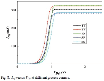
Fig. 9 shows that PSRR varies with frequency at four different Vdd cases. From the picture, when Vdd is 2.5 V, the PSRR achieves -100.3 dB at 100 Hz. Under the condition of Vdd = 1.5 V, the PSRR of the proposed VR is around -75.77 dB at 100 Hz.

Fig. 10 illustrates the simulation curves of PSRR versus frequency at different process corners when the supply voltage is 1.5 V. When the frequency is 100 Hz, the best and worst PSRR are -88.69 dB and -70.46 dB in FS and SF corners, respectively. Through the negative feedback technique, the variation of Irefis very small (see Fig. 8), the PSRR performance also benefits from this negative feedback structure.

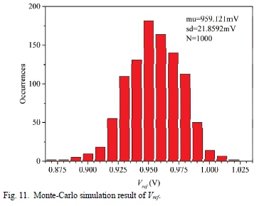
The sensitivity of the output reference voltage is evaluated by Monte Carlo simulation 1000 runs, which takes into account the effects of the mismatch and process variations in all the transistors of the proposed reference. When Vdd is 1.5 V, Monte-Carlo simulation result of Vrefat 27 °C is shown in Fig. 11. It can be clearly observed that the average value of Vrefis 959.121 mV, the standard deviation is 21.8592 mV, and the coefficient of variation σ/μ is about 2.27%.
From (12), we can see that TC of the proposed reference can become smaller by increasing K(mn3) and K(mn6) or decreasing K(mn4), K(mn5) and K(mn7). Besides, the PMOS current mirror uses the same large size transistors to reduce current mismatch and channel length modulation effects. As shown in Fig. 12, the PMOS current mirror occupies a large area in the layout. However, the VR circuit proposed in this paper is simple in structure and without using resistors and BJTs. Therefore, the final total layout area is only 0.0038 mm2 (66 μm * 58 μm).

The comparison of output voltage Vrefas a function of temperature between simulation and post layout simulation is shown Fig. 13. From the picture, we can know that the results of the simulation and post layout simulation only have a maximum difference of 0.054 mV, Therefore, the design of the circuit is reasonable.

The critical technical performances of the proposed voltage reference at five different process corners are shown in details in Table I. Under these five process corners, the worst TC, PSRR, LR are 23.3690 ppm/°C, -70.46 dB, 0.053 mV/V respectively. In addition, the maximum deviation of each performance is also very small. Therefore, the proposed circuit meets the design requirements. The characteristics of proposed circuit compared to other voltage reference circuits are shown in Table II where TC and PSRR of the proposed circuit are optimized, and the LR and area are significantly improved.
IV. CONCLUSION
This paper proposes a novel low LR CMOS voltage reference without BJTs and resistors, which is area efficient and less sensitive to temperature. The design is achieved by the TSMC 0.18 μm CMOS process. The output voltage with a low TC is obtained by utilizing output subcircuit composed of MOSFETs operating in the subthreshold region and saturation region. Through the use of the negative feedback technology, the amplifer is omitted, and the low LR can be realized. In the range of -20 to 110 °C, the proposed VR achieves TC of 18.6096 ppm/°C for a 1.5 V supply, while the PSRR is -75.77 dB at 100 Hz. The maximum variation of output voltage is only 0.037 mV from 1.5 V to 2.5 V supply voltage. The proposed VR with low TC, low LR, and high PSRR, can be attractive in high-precision systems.
REFERENCES
[1] A. Bendali and Y. Audet, "A 1-V CMOS current reference with temperature and process compensation," IEEE Transactions on Circuits and Systems I: Regular Papers, vol. 54, no. 7, pp. 1424-1429, Jul. 2007, doi: 10.1109/TCSI.2007.900176. [ Links ]
[2] A. Becker-Gomez, T. L. Viswanathan, and T. R. Viswanathan, "A low-supply-voltage CMOS sub-bandgap reference," IEEE Transactions on Circuits and Systems II: Express Briefs, vol. 55, no. 7, pp. 609-613, Jul. 2008, doi: 10.1109/TCSII.2008.921580. [ Links ]
[3] T. R. Perry, S. H. Lewis, A. P. Brokaw, and T. R. Viswanathan, "A 1.4 V supply CMOS fractional bandgap reference," IEEE Journal of Solid-State Circuits, vol. 42, no. 10, pp. 2180-2186, Oct. 2007, doi: 10.1109/JSSC.2007.905236. [ Links ]
[4] G. Bassi, L. Colalongo, A. Richelli, and Z. M. Kovacs-Vajna, "100 mV-1.2 V fully-integrated DC-DC converters for thermal energy harvesting," IET Power Electronics, vol. 6, no. 6, pp. 1151-1156, Feb. 2013, doi: 10.1049/iet-pel.2012.0625. [ Links ]
[5] K. Ueno, T. Hirose, T. Asai, and Y. Amemiya, "CMOS smart sensor for monitoring the quality of perishables," IEEE Journal of Solid-State Circuits, vol. 42, no. 4, pp. 798-803, Apr. 2007. doi: 10.1109/JSSC.2007.891676. [ Links ] [6] K. E. Kuijk, "A precision reference voltage source," IEEE Journal of Solid-State Circuits, vol. 8, no. 3, pp. 222-226, Jun. 1973, doi: 10.1109/jssc.1973.1050378. [ Links ]
[7] I. Lee, G. Kim, and W. Kim, "Exponential curvature compensated BiCMOS bandgap references," IEEE Journal of Solid-State Circuits, vol. 29, no. 11, Nov. 1994, doi: 10.1109/4.328634. [ Links ]
[8] K. M. Tham and K. Nagaraj, "A low supply voltage high PSRR voltage reference in CMOS process," IEEE Journal of Solid-State Circuits, vol. 30, no. 5, May. 1995, pp. 586-590, doi: 10.1109/4.384173. [ Links ]
[9] Y. H. Lam and W. H. Ki, "CMOS bandgap references with self-biased symmetrically matched current-voltage mirror and extension of sub-1-V design," IEEE Transactions on Very Large Scale Integration (VLSI) Systems, vol. 18, no. 6, Jun. 2010, pp. 857-865, doi: 10.1109/TVLSI.2009.2016204. [ Links ]
[10] Z. Y. Luo, Y. Lu, M. Huang, J. M. Jiang, S. W. Sin, U. Seng-Pan, and R. P. Martins, "A sub-1V 78-nA bandgap reference with curvature compensation," Microel ectronics Journal, vol. 63, May. 2017, pp. 35-40, doi: 10.1016/j.mejo.2017.02.016. [ Links ]
[11] Z. K. Zhou, Y. Shi, C. Gou, X. Wang, G. Wu, J. F. Feng, Z. Wang, and B. Zhang "A resistorless low-power voltage reference," IEEE Transactions on Circuits and Systems II: Express Briefs, vol. 63, no. 7, Jul. 2016, pp. 613-617, doi: 10.1109/TCSII.2016.2530096. [ Links ]
[12] Z. K. Zhou, P. S. Zhu, Y. Shi, H. Y. Wang, Y. Q. Ma, X. Z. Xu, L. Tan, X. Ming, and B. Zhang, "A CMOS voltage reference based on mutual compensation of Vtn and Vtp," IEEE Transactions on Circuits and Systems II: Express Briefs, vol. 59, no. 6, Jun. 2012, pp. 341-345, doi: 10.1109/TCSII.2012.2195065. [ Links ]
[13] H. Luo, Y. Han, R. C. C. Cheung, G. Liang, and D. Zhu, "Subthreshold CMOS voltage reference circuit with body bias compensation for process variation," IET circuits Devices & systems, vol. 6, no. 3, May. 2012, pp. 198-203, doi: 10.1049/iet-cds.2011.0170. [ Links ]
[14] T. N. Ghanavati, E. Farshidi, H. Sjoland, and A. Kosarian, "A high precision logarithmic-curvature compensated all CMOS voltage reference," Analog integrated circuits and signal processing, vol. 99, no. 2, pp. 383392, May. 2019, doi: 10.1007/s10470-018-1296-0. [ Links ]
[15] S. S. Chouhan and K. Halonen, "Design and implementation of a micropower CMOS voltage reference circuit based on thermal compensation of Vgs," Microelectronics Journal, vol. 46, no. 1, pp. 36-42, Jan. 2015, doi: 10.1016/j.mejo.2014.09.015. [ Links ]
[16] Q. L. Li, W. L. Deng, X. Y. Ma and J. K. Huang, "A novel low line regulation voltage reference with no amplifier," Journal of Circuits Systems and Computers, vol. 27, no. 10, pp. 1850152, Sep. 2018, doi: 10.1142/S0218126618501529. [ Links ]
[17] N. Alhassan, Z. Zhou, and E. S. Sanchez, "An all-MOSFET voltage reference with-50-dB PSR at 80 MHz for low-power SoC design," IEEE Transactions on Circuits and Systems II: Express Briefs, vol. 64, no. 8, pp. 892-896, Aug. 2017, doi: 10.1109/TCSII.2016.2614527. [ Links ]
[18] Y. T. Wang, Z. M. Zhu, J. J. Yao, and Y. T. Yang, "A 0.45-V, 14.6-nW CMOS subthreshold voltage reference with no resistors and no BJTs," IEEE Transactions on Circuits and Systems II: Express Briefs, vol. 62, no. 7, pp. 621-625, Jul. 2015, doi: 10.1109/TCSII.2015.2415292. [ Links ]
[19] K. Ueno, T. Hirose, T. Asai, and Y. Amemiya, "A 300 nW 15 ppm/degrees C, 20 ppm/ degrees C, 20 ppm/V CMOS voltage reference circuit consisting of subthreshold MOSFETs," IEEE Journal of Solid-State Circuits, vol. 44, no. 7, pp. 2047-2054, Jul. 2009, doi: 10.1109/JSSC.2009.2021922. [ Links ]
[20] Y. H. Zeng, Y. R. Huang, Y. L. Luo, and H. Z. Tan, "An ultra-low-power CMOS voltage reference generator based on body bias technique," Microelectronics Journal, vol. 44, no. 12, pp. 1145-1153, Dec. 2013, doi: 10.1016/j.mejo.2013.07.003. [ Links ]

Changqing Zhang received the B.A. degree from Hunan University of Science and Engineering, YongZhou, China, in 2017. He is currently pursuing the M.S. degree with Jinan University, Guangzhou, China. His current research interest includes the design of integrated circuit and system on chip.

Xia Wu received received the B.S. degree in electrical engineering from Jinan University, Guangzhou, China, in 1997 and the M.S. degree in education management from South China Normal University, Guangzhou, China, in 2009 respectively. Since 1997, she has worked in Jinan University. Her current research interests include semiconductor device physics and test methods.

Wanling Deng received the B.S. and Ph.D. degrees in electrical engineering from the South China University of Technology, Guangzhou, China, in 2003 and 2008, respectively. Since 2008, she has been an Associate Professor with the Department of Electronic Engineering, Jinan University, Guangzhou. Her current research interests include thin-film transistor (TFT) devices and physics, particularly poly-Si TFT and AOS TFT modeling.

Junkai Huang received the B.S. degree in applied physics and the M.S. degree in semiconductor device from Jinan University, Guangzhou, China, in 1985 and 1990, respectively, and the Ph.D. degree from the Institute of Microelectronics, South China University of Technology, Guangzhou, in 2011. He is currently a Professor with Jinan University. His current research interests include thin-film transistors' modeling, simulation, and integrated circuit design.

