


Services on Demand
Article
 English (pdf)
 Article in xml format
 Article references
Indicators

Related links
-
 Cited by Google
 -
 Similars in Google
Share

 Permalink
Journal of Energy in Southern Africa
On-line version ISSN 2413-3051
Print version ISSN 1021-447X
J. energy South. Afr. vol.29 n.1 Cape Town Feb. 2018
http://dx.doi.org/10.17159/2413-3051/2018/v29i1a1441
ARTICLES
Mitigating interference from switch-mode power supplies in sampling receivers
Muammar SlamdienII, *; Jacques WheelerI; Paul van der MerweII
IDepartment of Electrical, Electronic and Computer Engineering, Cape Peninsula University of Technology
IIReutech Radar Systems, a division of Reutech Pty Ltd
ABSTRACT
The research and development preliminaries, which led to an opportunity to embark on the present study took place during the system testing phase of a frequency-modulated continuous wave (FMCW) radar at Reutech Radar Systems, when a large false target was observed emerging on the range-Doppler map. The first indication was that the problem originated from interference caused by the switch-mode power supply (SMPS), which supplies direct current power to the radar receiver subsystem. This created the need for a new DC power supply, which was able to minimise the interference itself and mitigate the effects of the interference caused by the switching of the power supply. The present study is based on the research and development of techniques to mitigate interference from SMPS in sampling receivers, with emphasis on FMCW radar receiver applications. The study was divided into four main sections: research, simulation, design and evaluation. The research involved obtaining background information on sampling receivers, sampling theory, range-Doppler processing, SMPS, their effects, and mitigating these. This research section was utilised to simulate the various interference mitigation techniques, while a power supply printed circuit board (PCB) was established in the design phase to practically illustrate the techniques being utilised. Lastly, during evaluation, this PCB was evaluated against the criteria set out in the research phase. The results demonstrated that the techniques of synchronising the pulse width modulation clock to the sampling frequency and sweep repetition frequency yielded a significant reduction in the SMPS noise on the range-Doppler map. This technique may also be applied in other electronic sampling systems which perform digitisation of the input data, such as analogue-to-digital converters.
Keywords: radar, FMCW, SMPS, range-Doppler processing
1. Introduction
During the system testing phase of a frequency-modulated continuous wave (FMCW) radar at Reutech Radar Systems (RRS) in 2013, a large false target emerged clearly on the range-Doppler map (RDM) after the range-Doppler processing of the radar data. After many weeks of relentless troubleshooting, it became apparent that the problem originated from interference caused by the switchmode power supply (SMPS), which supplies DC power to the radar receiver subsystem. This established the research opportunity to design, manufacture, test and integrate a new DC power supply for the radar receiver subsystem, specifically for use in a portable radar system. The main challenge was to develop a design methodology or approach which will enable conformance to all the electrical requirements for the power supply, while at the same time minimising loss of integrity in the final sampled signal.
The DC power supplies, which comply with military specifications and can conform totally to industry's electrical and mechanical requirements, are typically not available off-the-shelf. A custom printed circuit board (PCB) therefore needed to be developed according to this methodology for this application. This custom PCB must be developed to effectively mitigate the adverse effects induced by the SMPS without compromising its functionality or reliability. In FMCW radar, for example, this will result in the minimum loss of sensitivity at certain (affected) target ranges/velocities, hence making a much more effective and sensitive radar system.
The research questions were as follows:
a) Can the unit be effectively integrated with the
receiver subsystem?
• the unit must provide the required voltage and load current for the receiver subsystem;
• the efficiency of unit must be equal to or better than a typical off-the-shelf SMPS.
b) Can a DC power supply PCB be developed which mitigates the effects of the SMPS?
• the PCB must greatly reduce the SMPS electromagnetic interference (EMI), by producing a clean, synchronous output;
• the PCB must be able to minimise the processed radar data distortion, due to the SMPS switching frequency and its harmonics, when viewed by real-time spectrum analysis;
• the PCB must be able to eliminate 'false targets' on the RDM caused by the SMPS frequency.
(c) Can the PCB be designed to comply with military and industry specifications?
• the PCB must be designed according to military specifications;
• the PCB must be designed according to industry specifications.
2. Literature review
The technologically advanced world has expanded applications for sampling receivers from radar systems to communications receivers, test and measurement equipment, and wireless infrastructure equipment. The technique can even be used for medical imaging applications (Texas Instruments Inc, 2011). In the majority of applications, minimum interference is required for maximum accuracy, which makes mitigating SMPS interference critical (Texas Instruments Inc, 2011). Frequency-modulated continuous wave radar receivers were reviewed, as a typical application for a sampling receiver.
2.1. Frequency-modulated continuous wave radar and sampling receivers
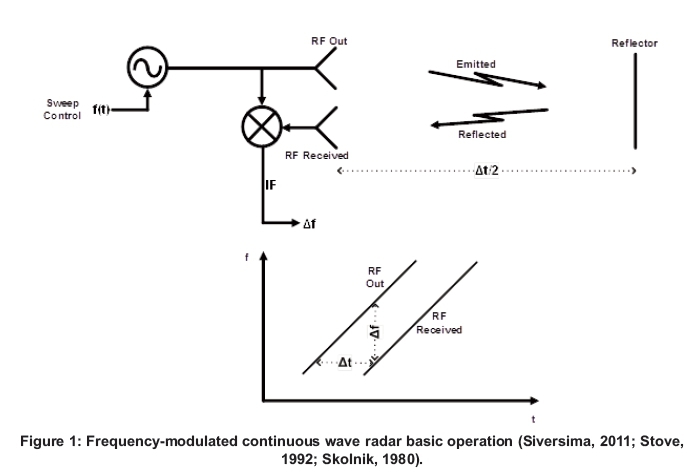
A full understanding of the radar sampling receiver subsystem and its power supply starts with an examination of the entire system, from its basic operating principles, as illustrated in Figure 1 (Siversima, 2011; Stove, 1992; Skolnik, 1980).
The frequency of the transmitted signal is modulated over time, while keeping constant amplitude, thus generating a linear frequency sweep across a pre-determined bandwidth. The simplest and most commonly used frequency modulation pattern for the transmitted signal is the saw-tooth function. The transmitted radio frequency (RF) signal will be reflected off the target, back to the radar (Siversima, 2011; Griffiths, 1990). The reflected RF signal received by the radar will be a replica of the transmitted signal, delayed by the propagation delay (two ways). The propagation delay is given by Equation 1.
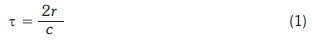
where r is the target range, and c is the wave propagation velocity in air.
The received RF signal is then mixed with the transmitted signal, producing a new signal, which indicates the difference in frequency between the received and transmitted signals. The instantaneous difference in frequency, Af, will be in the low frequency or intermediate frequency (IF) range and may be used to determine the target's range (Griffiths, 1990; Siversima, 2011).
The primary function of an FMCW radar sampling receiver is to receive the reflected RF signal from the target (via the antenna). This received RF signal will then be mixed with the transmitted RF signal, to produce Af. More critical, though, is that the radar sampling receiver can detect these reflected RF signals from the target in the presence of interference, noise and clutter. The receiver must not only filter out the unwanted signals, but also amplify the desired ones for signal processing. The requirement to provide sufficient gain, phase and amplitude stability, dynamic range and be as robust as possible makes receiver design very complicated (Griffiths, 1990; Skolnik, 1980).
X-band frequencies are usually used for FMCW radar. At X-band, the external noise entering via the antenna is quite low, making the internal noise generated by the receiver (and the rest of the radar) itself the main issue to focus on. The primary objective is to maximise the signal-to-noise ratio of the receiver output signal. To achieve this, a matched filter is utilised, which produces the required frequency response of the IF (output) section of the receiver (Skolnik, 1980; Ponsford, 1988).
2.2. Power supply
It was necessary to determine whether to use a linear or SMPS for the application in this section. The operation principle of the selected power supply and the best topology for the application are discussed, as well as possible effects (interference) caused by the power supply, along with their mitigation techniques.
The use of a linear power supply will eliminate the interference created by a SMPS. The disadvantage of a linear power supply is that it dissipates an excessive amount of power, which makes it inherently inefficient. This excessive power dissipation also causes excessive heat dissipation, which may force the addition of a heatsink, causing an increase in the size of the power supply. The use of a high-efficiency and compact SMPS is preferable, in order to meet the portable radar system requirements (Teodorescu & Brezeanu, 2014; Linear Technologies, 2013; Kuo-Bin et al., 1999; Brown, 1990; Dunfan et al., 2011).
The research found that using a basic buck converter topology was best suited for the application, mainly because of its very high efficiency, few components, and lack of magnetic elements, which makes it compact in size and inexpensive to develop (Teodorescu & Brezeanu, 2014; Linear Technologies, 2013).
2.3. Switch-mode power supply effects and effects mitigation
Energy at the SMPS fundamental frequency, as well as several of its harmonics, propagates (via conduction) onto electrical interconnecting harnesses, and thus get transferred between subsystems (Chand & Sathyanarayanan, 2006; Mee & Teune, 2002).
Switch-mode power supply generally operates in the IF range, and the desired output frequencies of the receiver subsystem are also in this frequency range. This means that the receiver matched filter will not filter out SMPS interference. The receivers also incorporate a substantial amount of gain at these frequencies (to increase sensitivity), and this gain is increased even further during signal processing. In an FMCW radar system, a constant frequency in the IF band will be interpreted as a target by the signal processor. In the case that the switching interference is interpreted as radar data, the 'false' target has the potential to mask a 'real' target, if they are in close proximity on the RDM. This is highly undesirable, and it is thus imperative to mitigate the switching interference (van der Merwe, 2015; Ho-En et al., 2013).
Various techniques that may be used to mitigate the effects of SMPS on sampling receivers were reviewed. The best techniques were found to be synchronisation of the SMPS to the sample frequency and synchronisation to the sample repetition frequency (SRF).
2.3.1. Synchronising to the sample frequency
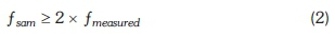
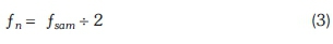
The idea in this technique is to synchronise the SMPS frequency to the sampling frequency of the receiver subsystem (or a multiple thereof), aiming to effectively 'hide' the SMPS frequency after it has been sampled (digitised) by the receiver's analogue-to-digital converter (ADC). This approach has previously been used in audio and other systems to prevent unwanted mixing products and interference (Pefhany, 2014). It is important to first understand the basics of sampling theory. Firstly, the Nyquist sampling theorem states that the sampling frequency should be at least twice the frequency being measured to avoid aliasing, as shown in Equation 2.
The Nyquist frequency is given by Equation 3.
(Olshausen, 2000; National Instruments, 2016).
Aliasing can be explained through a practical example. If the sample frequency is 2 kHz, this gives a Nyquist frequency of 1 kHz. If a measured frequency is 0.75 kHz, the Nyquist sampling theorem will be satisfied, and the digitised resultant frequency will be given by Equation 4.
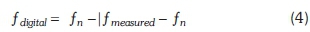
which is 0.75 kHz in this case (Olshausen, 2000; Indiana University, 2013).
If the Nyquist sampling theorem is not satisfied, on the other hand, and a frequency of 1.5 kHz is measured, the digitised resultant frequency will be 0.5 kHz. In this case, the signal has aliased around the Nyquist frequency according to Equation 4 (Olshausen, 2000; Indiana University, 2013).
This literature shows that, theoretically, if the SMPS frequency is equal to the sampling frequency of the receiver subsystem (or a multiple thereof), it should aliase back to 0 Hz (DC) after digitisation, according to Equation 4. This makes this technique extremely desirable, as it will effectively 'hide' the SMPS frequency after it has been sampled, hence mitigating the interference caused by the SMPS (National Instruments, 2016; Indiana University, 2013).
Implementing this approach, a synchronous buck converter package will be needed. This technique will also only be relevant when the sampling frequency is lower or equal to the switching frequency. The problem is that in some cases the switching frequency cannot be controlled to be a multiple of the sampling frequency because the sampling frequency is often higher than typical switching frequencies.
2.3.2. Synchronising to the sweep repetition frequency
The SRF is typically much lower than the sample frequency, so that when synchronising the SMPS frequency to the SRF of the signal processor synchronisation is much easier. This approach has been used previously in many wireless communication systems, not necessarily for SMPS synchronisation, but for the synchronisation of other subsystems to prevent signal processing errors caused by interference (Salous, 2008). To grasp this concept, one needs to understand the basics of the range-Doppler processing (RDP) performed by the signal processor of FMCW radar systems. Generally, how RDP works is that two fast Fourier transforms (FFTs) are applied to the receivers output signal. The first is the range FFT, to determine the target's range. The second is the Doppler FFT, to determine the targets velocity. The velocity is calculated by the change in phase of the target, i.e. zero change means the target is stationary (Aljasmi, 2002). Essentially, it is desired that the SMPS frequency is synchronised to the SRF of the Doppler FFT. This means that every time the sweep is performed the phase of the SMPS frequency will remain unchanged (zero phase-shift) relative to the sweep repetition frequency of the Doppler FFT. This approach produces a predictable response (stationary target in FMCW systems). This stationary target may then be filtered out (along with other stationary targets and noise) in the post-processing filtering (van der Merwe, 2015; Deacon et al., 2011).
The application of this approach requires also using a synchronous buck converter package will also be utilised. This technique may also be used in conjunction with the technique of synchronisation to the sample frequency and can thus be considered to be suitable for the application, as it would also effectively 'hide' the SMPS frequency on the RDM.
2.3.3. Printed circuit board design considerations
According to Mee & Teune (2002), Chand & Sathyanarayanan (2006) and Linear Technologies (2009), the conducted EMI of a SMPS may be greatly reduced by giving special attention to the following:
• minimising loop areas in the PCB layout;
• reducing the parasitic inductance and capacitance by careful placement of components;
• ensuring sufficient filtration of the input and output;
• using low ESR capacitors for input and output filtration;
• minimising trace inductance (avoid unnecessarily long tracks);
• segregating the signal ground, power ground and GND return layers; and
• using ground pours (flood) all unused areas with copper on all the layers.
2.4. Sampling theory
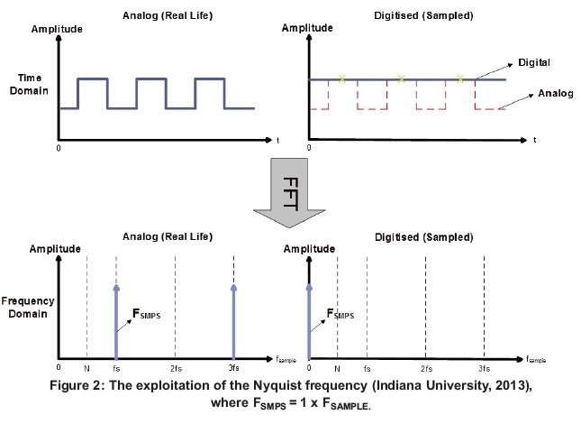
This section provides some background on sampling theory, as well as a graphical illustration of the application of the technique, in order to understand the technique of synchronising the SMPS to the sampling frequency. Figure 2 shows a typical switching signal from a SMPS - a square wave. It illustrates this signal in analogue form and after digitisation, in both the time and frequency domains. The top left graph in the figure shows the signal in analogue and the top right graph shows the same signal after digitisation (both in the time domain), in this case:
The sampled result is DC or 0 Hz (van der Merwe, 2015; Indiana University, 2013).
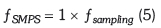
The bottom panels of Figure 2 show the frequency domain after an FFT was applied. Here, Equation 5 is clear, and the harmonics generated, will naturally be at 3 χƒ sampling and 5 χƒ sampling etc. This means the harmonics will also be a multiple of the sampling frequency, and hence, all these frequencies will aliase to DC or 0 Hz, as can be seen in the bottom right panel. This effectively 'hides' the SMPS frequency for sampling receiver applications, and makes the technique ideal for application in the present study (van der Merwe, 2015).
2.5. Range-Doppler processing
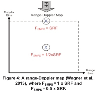
This section provides some background on RDP, as well as a graphical illustration of the application of the technique, in order to understand the technique of synchronisation of the SMPS to the SRF. Figure 3 shows the RDP of raw radar data from the receiver subsystem. At this point, another FFT is performed, and the resultant RDM can be seen in Figure 4. The top panel in Figure 3 illustrates how the phase of Af from the radar receiver subsystem changes as a target approaches or moves away from the radar. After a (horizontal) range FFT is applied to the top panel, the bottom panel is obtained. The bottom panel then also illustrates this phase shift (sweep by sweep), as a clockwise or anti-clockwise rotation of the arrows.
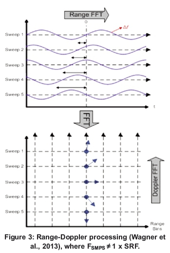
This means that when an asynchronous SMPS switching frequency filters through to signal processor, it will be interpreted as moving target, as every time a sweep is performed, it will sample the SMPS switching frequency at a 'random' phase (Aljasmi, 2002; van der Merwe, 2015; Wagner et al., 2013).
If, however, the SMPS switching frequency is synchronised to the SRF, the sweep will sample the SMPS switching frequency at the same phase continuously. This approach causes the SMPS switching frequency to be interpreted as a stationary target, at the edge of the RDM, which is a much more desirable and predictable outcome, as it will always appear at the same location on the RDM (rather than continuously hopping around). This can be seen in Figure 4, which shows a typical RDM (van der Merwe, 2015; Wagner et al., 2013).
From literature, the use of this method is considered suitable for the portable radar application, as it interprets the SMPS frequency as a stationary target, at the edge of the RDM, and effectively mitigates the effects of the SMPS interference.
2.6. Industry and military compliance
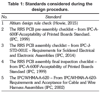
Compliance to industry and military specifications will be achieved with the implementation of certain procedures and checks. For the PCB design, RRS utilises the Altium design rule check. This is a powerful feature which verifies that the logical and physical integrity of the design is compliant to industry and military specifications (Howie, 2015). The Institute for Interconnecting and Packaging Electronic Circuits (IPC) standards provide the best practices for the electronics industry and give guidelines for the entire supply chain. These standards are accepted worldwide as the benchmark specification for aerospace, industry and military grade electronic products; hence the IPC standards are used by RRS as a guideline to design and build in compliance with military and industry specifications (IPC, 2016).
All the specifications (standards) mentioned in Table 1 were adhered to strictly, in order to ensure that the final product of the power supply unit (PSU) design is fully compliant to industry and military specifications.
2.7. Literature review conclusion
Based on literature reviewed, the SMPS with the basic buck converter topology is deemed the best solution. Mitigation of SMPS interference is found to be critical for sampling receivers and FMCW radar applications. The bulk of the interference is deemed to be from the switching of the SMPS itself. The best approach to minimise the interference is to give special attention to the PCB layout, as well as either making sure, when switching f > sampling f, that switching frequency is a multiple of the sampling frequency, or that it is synchronised to the SRF. The application of both techniques simultaneously should, theoretically, yield the best outcomes, because the 'false target' will then be stationary in range and Doppler. Lastly, all the Altium design rule checks and IPC specifications will be followed strictly to ensure that the design of PCB is industry and military compliant.
3. Simulation
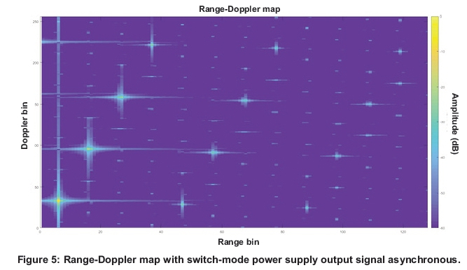
The two interference mitigation approaches - synchronising the SMPS frequency to a multiple of the sampling frequency and synchronising it to a multiple of the SRF - are evaluated in this section by means of simulation, using Matlab-2015. Figure 5 shows the RDM with the SMPS frequency asynchronous relative to the sample frequency and SRF of the radar signal processor. From the graph it can be seen that, after a range and Doppler FFT was performed, the SMPS frequency and its harmonics are interpreted as moving targets on the RDM. This desensitises the radar completely, as one is not able to distinguish between real and false targets.
From Figure 5, it can be seen that, after a range and Doppler FFT was performed, the SMPS frequency and its harmonics are interpreted as moving targets on the RDM. This desensitises the radar completely, as one is not able to distinguish between real and false targets.
With the SMPS frequency equal to a multiple of the SRF, the SMPS frequency and its harmonics were no longer interpreted as moving targets on the RDM, but could be seen at zero-Doppler at various range bins. Since they are at zero-Doppler, it means they will be interpreted as stationary targets, which are filtered out during signal processing, meaning it is not a problem for radar applications.
Synchronising to the sample frequency should, however, shift the interference to range-bin 0 as well. To eliminate the targets at zero-Doppler, we must ensure that the SMPS frequency is equal to both a multiple of the SRF and a multiple of the sampling frequency. The results of the simultaneous implementation of both approaches are shown in Figure 6.
The simulation in Figure 6 shows that the simultaneous implementation of both approaches (synchronising to a multiple of the sampling frequency and SRF) yields no false targets at all. The application of both techniques in a real SMPS (simultaneously) should thus provide the required interference mitigation for the application.
4. Design specification
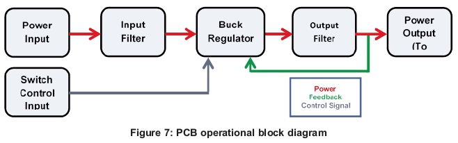
The main aspects of the design specification are outlined in this section, and include the receiver subsystem integration, SMPS interference mitigation, and military and industry compliance. Figure 7 shows the operational block diagram of the PCB for a more holistic view of the design. The main aspects of the design specification are highlighted in the sub-sections which follow.
4.1 Receiver subsystem integration
• The radar power distribution unit shall provide 108 mA at 12 V DC (nominal) to the input of
the SMPS PCB.
• A power connector interface shall be incorporated on the SMPS PCB to connect to the radar power distribution unit.
• The buck regulator shall down-convert the 12V 108 mA input to a 5.4V 200 mA output (nominal).
• The output rise time (time to complete the transient phase) shall be less than or equal to 6 ms.
• A feedback mechanism shall be implemented to ensure output regulation.
• The efficiency of the converter shall be better than 90%.
4.2 Switch-mode power supply interference mitigation
• For the input filter a common mode filter shall be incorporated, along with a low-pass filter circuit, to ensure that the input power to the SMPS PCB is as clean as possible.
• The switch-control input shall provide an input clock signal for the buck regulator to synchronise to.
• This switch-control input signal shall be sourced either from the radar receiver subsystem or signal processor.
• The RF SMA connector interface shall be incorporated on the SMPS PCB to connect to the switch control input.
• The buck-regulator shall be able to synchronise its switching frequency to the switch control input (to implement the interference mitigation techniques).
• For the output filter, a low-pass filter circuit should be incorporated, to minimise the output voltage ripple and ensure that the output power to the load is as clean as possible.
4.3 Military and industry specification compliance
• The Altium design rule check shall be enforced to ensure compliance to military and industry tolerances and clearances.
• The RRS PCB pre-assembly checklist shall be used to verify that the bare PCB is manufactured and delivered as per the quality control PCB workmanship inspection criteria from IPC-A-600F - acceptability of printed boards standard and thus also compliant with military and industry specifications (IPC, 1999).
• The RRS PCB assembly checklist shall be used to verify that the PCB is assembled according to IPC-J-STD-001E - requirements for soldered electrical and electronic assemblies, and hence also compliant with military and industry specifications (IPC, 2014).
• The RRS PCB assembly final inspection checklist shall be used to verify that the PCB workmanship follows the inspection criteria from IPC-A-600F - acceptability of printed boards standard, and subsequently with military and industry specifications (IPC, 1999).
• The IPC/WHMA-A-620 - requirements and acceptance for cable and wire harness assemblies shall be used to verify that the system integration harnesssing has been done according to IPC, military and industry specifications (IPC, 2002).
5. Design procedure
This section discusses the PCB schematic circuit design and simulation and outlines the PCB layout and assembly procedures, including its final inspection.
5.1. Circuit design and simulation
This section covers the buck converter selection and PCB schematic design. The results of the simulation of the design, using the LTspice software is also included here. The buck converter integrated circuit requires an efficiency equal to or better than a typical off-the-shelf SMPS, which is approximately 90%. Because of its very high efficiency and availability in RRS's stores, the LTC3601 has been found to be the package best suited to this application (Huffman, 1991). Once the component values are calculated for the LTC3601, the next step is to do the schematic design, using Altium designer software.
Using LTspice simulation software, it is possible to accurately predict the characteristics of the circuit. This tool is used to verify that the circuit performs all the required functions. The output rise time and synchronisation to the sync input is also verified. According to the simulation, with an input voltage of 12 V, the circuit produces an output of 5.38 V (target 5.4V), with an output rise time of 4.4 ms (target less than 6 ms), this is a desirable result. The simulated output current is equal to 198.89 mA. Since the target output current is 200 mA, the result is satisfactory for the required application. From the simulation, it was also observed that the switching output is synchronised to the synchronisation input at a frequency of 976 kHz. This result is desirable.
5.2. Printed circuit board layout, manufacture and assembly
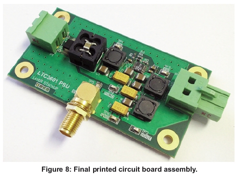
This section documents the PCB layout procedure, including the provisional layout, routing, manufacture, and inspection procedures. The provisional component layout was first done, using the Altium designer software. The routing was then completed, and the layout and routing PCB design EMI mitigation techniques application was successfully verified. The PCB assembly data-pack was compiled and then thoroughly scrutinised in the design reviews. Once the data-pack was approved, it was sent for manufacture. Post-delivery, the bare PCB is inspected (pre-assembly checklist), the components can then be soldered on to it, and this is referred to as the PCB Assembly. The PCB was assembled according to the standard IPC-J-STD-001E -requirements for soldered electrical and electronic assemblies (IPC, 2014). Figure 8 shows the completed PCB assembly, with all the components and interfaces populated. Next, it was successfully verified that the PCB was assembled according to the standard IPC-J-STD-001E - requirements for soldered electrical and electronic assemblies (IPC, 2014). The PCB now underwent a final inspection as per the QC PCB workmanship inspection criteria from IPC-A-600F-Acceptability of Printed Boards Standard (IPC, 1999). Since all the criteria complied, the PCB could now be evaluated.
6. Experimental evaluation
This section states the answers to the research questions: whether the goals were achieved and why. A summarised version of the results and observations will be provided for each section.
6.1. Receiver subsystem integration evaluation
The PSU was evaluated on the bench, in isolation, for this test. The PSU PCB was found to be in full compliance with voltage, current, and efficiency requirements for the receiver subsystem integration; it was then deemed safe to commence receiver subsystem integration.
6.2. Interference mitigation evaluation
Once the receiver subsystem integration evaluation was completed, the PSU PCB was integrated with the radar receiver subsystem. The purpose of the integration is evaluation of the interference mitigation techniques implemented in the PCB design. The output of the PSU PCB was found to be clean and, because it was able to synchronise to both the sample frequency and the SRF, the PSU PCB was considered to be capable of significantly reducing the SMPS EMI through the production of clean, synchronous output. The synchronisation evaluation was, therefore, deemed successful.
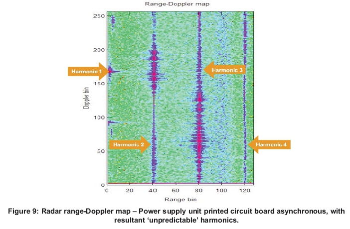
The core of the present study eventually comes down to how clean the RDM is. For this reason, the RDM with and without the interference mitigation techniques implemented was evaluated. Figure 9 shows that, with the PSU PCB asynchronous, there is interference caused by the SMPS frequency and its harmonics around range bin 5, 40, 80 and 120. The interference viewed is aliased ('folded-back') harmonics of the asynchronous SMPS carrier frequency. Due to the asynchronous nature of the SMPS, the resultant harmonics are 'unpredictable'.
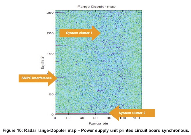
Additionally, the reason that the interference seems to be 'smudging' on the RDM is because of the SMPS being in burst-mode. Burst-mode causes the SMPS carrier frequency and subsequently its harmonics, to be unstable and constantly vary in frequency (range) and Doppler (velocity). Figure 10 shows the radar RDM with the PSU PCB synchronised.
Figure 10 shows that, with the PSU PCB synchronised, the interference caused by the SMPS frequency and its harmonics have now been dramatically reduced, for the following reasons:
• synchronising to the sample frequency causes the interference frequencies to aliase to 0 Hz, i.e. in range bin 0;
• synchronising to the SRF causes the interference frequencies to be in phase with the SRF and hence fall into Doppler bin 0.
The following observations were made that would not have been seen in the simulation in Figure 6:
• the system clutter 1 is because there is no target (large peak) being sensed by the radar, this then increases the radar sensitivity, which enhances ambient noise;
• the system clutter 2 is inherent system noise. The mean of the system noise is very close to 0, thus placing it in Doppler bin 0; and
• the minor SMPS interference is due the SMPS output frequency jitter. For the current application, the radar will not be looking at very close in targets; hence, the desensitisation below Range bin 20 does not affect the system integrity, which is still acceptable.
The PSU PCB was thus able to successfully eliminate majority of the 'false targets' on the RDM caused by the SMPS frequency. The system clutter encountered and the minor SMPS interference were deemed acceptable.
6.3. Military and industry compliance evaluation
The evaluation for military and industry specification compliance was conducted at a PCB and schematic level, Altium design rule check was utilised, and at an assembly level IPC soldering and harnessing standards were followed. The results of the verification of these procedures can be seen in Table 2, which shows that the PSU PCB design passed the Altium design rule check. The assembly procedure was done according to IPC standards, and the receiver subsystem integration harnessing also followed IPC protocol (IPC, 2014; IPC, 2002).
7. Conclusions
The power supply unit (PSU) printed circuit board (PCB) was found to be in compliance with voltage and current requirements for the receiver subsystem integration. The efficiency was determined to be 92.31%, which is better than the 90% for a typical off-the-shelf switch-mode power supply (SMPS).
The measured output of the PSU PCB was found to be clean, and because it was able to synchronise to both the sample frequency and the sample repetition frequency (SRF), it can be concluded that the PSU PCB is able to greatly reduce the SMPS electromagnetic interference, by producing a clean, synchronous output.
When the PSU PCB is synchronised to the sample frequency and SRF, with the synchronising clock (SYNC CLK) connected, the PSU PCB is able to minimise all processed radar data distortion (while viewed by real-time spectrum analysis), caused by the SMPS switching frequency and its harmonics.
The PSU PCB was able to successfully eliminate the majority of the 'false targets' on the range-Doppler map caused by the SMPS frequency. The system clutter encountered was as expected, and the minor SMPS interference was deemed acceptable. The SMPS jitter interference mitigation was beyond the scope of this study, but it showed itself to be a feasible area for future research.
The PSU PCB was found to be compliant with the Altium design rule check and IPC standards. Since these are accepted worldwide for aerospace, industry and military grade products, we can conclude that the PSU PCB was designed and built in compliance with military and industry specifications (IPC, 2016).
The buck converter (LTC3601) has a maximum switching frequency of 4MHz, in future, for applications with higher sampling frequencies, an alternative converter with a higher switching frequency should be considered (Linear Technologies, 2009).
The approach developed in this study, i.e. to synchronise the PSU to a system SYNC CLK, may in future be utilised to synchronise other interference generating radar sub-systems such as the Ethernet clock etc.
The technique may also be applied outside of radar systems, in other electronic sampling systems which perform digitisation of the input data. Some examples are vector network analysers, spectrum analysers, oscilloscopes, and many other types of electronic equipment which use analog-to-digital converters.
References
Ponsford, A. M. and Bagwell, D. J., 1988. Receiver design for high frequency ground-wave radar. London, Fourth International Conference on HF Radio Systems and Techniques: 254-258. [ Links ]
Aljasmi, R., 2002. Frequency modulated continuous wave-radar signal processing and parameter estimation, Linköping: Swedish defence reseacrch agency. [ Links ]
Brown, M. C., 1990. Practical switching power supply design. 1 ed. s.l.: Academic Press, Inc. [ Links ]
Dunfan Y., Xifeng W., Dongwei L., Y ongguang Z. and Shunming S., 2011. Design of a low-cost and high-performance direct current linear power supply using in electronic experiment, Heilongjiang, 2011 Cross Strait Quad-Regional Radio Science and Wireless Technology Conference, Vol. 2:1103-1106 . [ Links ]
Griffiths, H. D., 1990. New ideas in frequency modulated radar. Electronics & Communication Engineering Journal 2(5): 185-194. [ Links ]
Ho-En L., Guan-Yu L., Ming-Hwa S., Siang-Min S. and Sin-Siang W., 2013. A computation efficiency andconstant false alarm rate. Beijing, 2013 Ninth International Conference on Intelligent Information Hiding and Multimedia Signal Processing: 108-112. [ Links ]
Howie, J., 2015. Design Rule Checking. [Online] Available at: https://techdocs.altium.com/display/ADOH/Design+Rule+Checking [Accessed 31 March 2016]. [ Links ]
Huffman, B., 1991. Efficiency and power characteristics of switching regulator circuits. [Online] Available at: http://cds.linear.com/docs/en/applica-tion-note/an46.pdf [Accessed 15 October 2015]. [ Links ]
Indiana University, 2013. Nyquist theorem and aliasing. [Online] Available at: http://www.indiana.edu/~emusic/etext/digital_audio/ chapter5_nyquist.shtml [Accessed 30 March 2016]. [ Links ]
Institute for Interconnecting and Packaging Electronic Circuits (IPC), 1999. IPC-A-600F. F ed. Northbrook: IPC. [ Links ]
Institute for Interconnecting and Packaging Electronic Circuits (IPC), 2002. IPC/WHMA-A-620 -Requirements and acceptance for cable and wire harness assemblies. [Online] Available at: http://www.ipc.org/TOC/IPC-A-620.pdf [Accessed 05 October 2015]. [ Links ]
Institute for Interconnecting and Packaging Electronic Circuits (IPC), 2014. IPC-J-STD-001E -Requirements for soldered electrical and electronic assemblies. E ed. s.l.:IPC. [ Links ]
Institute for Interconnecting and Packaging Electronic Circuits (IPC), 2016. IPC - Association connecting electronics industries - Overview document. [Online] Available at: http://www.ipc.org/2.0_IPC/2.1_About/pdfs/IPC_Overview.pdf [Accessed 28 February 20157]. [ Links ]
Kuo-Bin L., Chen-Yao L. and Jeng-Tzong S., 1999. High efficiency linear power supply with a preregulator controlled by keeping constant Rds of MOSFET. New York, Proceedings of the 1999 Particle Acellerator Conference, Vol. 5: 3776-3778. [ Links ]
Teodorescu, L. and Brezeanu, G., 2014. High efficiency low noise linear power supply for high power measurement systems. Bucharest, 2014 International Symposium on Fundamentals of Electrical Engineering: 1-5. [ Links ]
Linear Technologies, 2009. LTC3601 15V Monolithic synchronous step-down regulator. [Online] Available at: http://cds.linear.com/docs/en/datasheetZ3601fc.pdf [Accessed 28 February 2017]. [ Links ]
Linear Technologies, 2013. Basic concepts of linear regulator and switching mode power supplies. [Online] Available at: http://cds.linear.com/docs/en/application-note/AN140fa.pdf [Accessed 28 January 2014]. [ Links ]
Mee, S. W. and Teune, J. E., 2002. Reducing emissions in the buck converter switch-mode power supply. Minneapolis, Electromagnetic Compatibility, 2002. IEEE International Symposium, Vol. 1: 179-183. [ Links ]
National Instruments, 2016. Aliasing and sampling at frequencies above the nyquist frequency. [Online] Available at: http://www.ni.com/white-paper/3000/en/ [Accessed 31 March 2016]. [ Links ]
Olshausen, B. A., 2000. Aliasing. [Online] Available at: http://redwood.berkeley.edu/bruno/npb261/aliasing.pdf [Accessed 30 March 2016]. [ Links ]
Pefhany, S., 2014. What benefit is there in synchronizing my switching supply to the system clock. [Online] Available at: http://electronics.stackexchange.com/questions/97865/what-benefit-is-there-in-synchroniz-ing-my-switching-supply-to-the-system-clock [Accessed 31 March 2016]. [ Links ]
Deacon, P, Hunt, R, Koenigsknecht, D, Leonard, C and Oakley, C., 2011. Frequency modulated continuous wave radar. [Online] Available at: http://www.egr.msu.edu/classes/ece480/capstone/fall11/group06/styl e/Technical%20Presentation.pdf [Accessed 31 March 2016]. [ Links ]
Salous, S., 1986. Frequency modulated continuous wave channel sounder with digital processing for measuring the coherence of wideband high frequency radio links. Communications, Radar and Signal Processing, IEE Proceedings F 133(5): 456-462. [ Links ]
Siversima, 2011. Frequency modulated continuous wave radar sensors. [Online] Available at: http://www.siversima.com/wp-conten/uploads/2011/06/FMCW-Radar-App-Notes-Frequency-Modulated-Continuous-Wave-Radar.pdf [Accessed 20 January 2015]. [ Links ]
Skolnik, M. I., 1980. Introduction to radar systems. 2nd ed. s.l.: McGraw-Hill. [ Links ]
Stove, A., 1992. Linear Frequency Modulated Continuous Wave radar techniques. Radar and Signal Processing, IEE Proceedings F 139: 343-350. [ Links ]
Chand, S. and Sathyanarayanan, A., 2006. Emission analysis & compliance practices of switch-mode power supplies. Bangalore, 9th International Conference on Electromagnetic Interference and Compatibility: 189-194. [ Links ]
Texas Instruments, 2011. Intermediate frequency sampling receiver concepts. [Online] Available at: http://www.ti.com/lit/wp/snaa107/snaa107.pdf [Accessed 2 February 2015]. [ Links ]
Wagner, T, Feger, R and Stelzer, A., 2013. Wide-band range-doppler processing for frequency modulated continuous wave systems. Nuremberg, 2013 European Radar Conference: 160-163. [ Links ]
Van der Merwe, P J., 2015. [Interview] (10 March 2015). [ Links ]
* Corresponding author: Tel: +27 21 880 1150. Email: muammars@mweb.co.za

