


Servicios Personalizados
Articulo
 Inglés (pdf)
 Articulo en XML
 Referencias del artículo
Indicadores

Links relacionados
-
 Citado por Google
 -
 Similares en Google
Compartir

 Permalink
South African Journal of Science
versión On-line ISSN 1996-7489
versión impresa ISSN 0038-2353
S. Afr. j. sci. vol.106 no.11-12 Pretoria nov./dic. 2010
http://dx.doi.org/10.4102/sajs.v106i11/12.297
RESEARCH LETTER
The influence of deposition temperature on vanadium dioxide thin films microstructure and physical properties
Velaphi MsomiI; Oaisin NemraouiII
IDepartment of Mechanical Engineering, Cape Peninsula University of Technology, Cape Town, South Africa. email: msomiv@gmail.com
IIDepartment of Physics, University of Zululand, South Africa
ABSTRACT
Vanadium dioxide thin films were successfully prepared on soda lime glass substrates using the optimised conditions for r.f-inverted cylindrical magnetron sputtering. The optimised deposition parameters were fixed and then a systematic study of the effect of deposition temperature, ranging from 450 ºC to 550 ºC, on the microstructure of thermochromic thin films was carried out. The deposited films were found to be well crystallised, showing strong texture corresponding to the (011) plane, indicating the presence of vanadium dioxide.
Keywords: deposition temperature; microstructure; thermochromism; thin films; vanadium dioxide
INTRODUCTION
Vanadium dioxide (VO2) is an interesting material because of its transition from semiconducting to metallic behaviour at a transition temperature of about 70 ºC.1 This behaviour is accompanied by a microstructural change from a monoclinic (below transition temperature) to a tetragonal structure (above transition temperature).2 VO2 has a narrow band gap (0.65 eV) below the transition temperature.3,4 Numerous researchers5,6,7 have reported that VO2 phase change is accompanied by an abrupt change in the electrical resistance and optical transmittance. It has low transmittance around the infrared region during the metallic phase and has higher transmittance in the infrared region during the semiconducting phase. As a result of this behaviour, VO2 has been of interest for various applications, such as the 'smart window', laser protection and electrical auto-switching. The transition temperature (~70 ºC) can be decreased or increased using dopants (e.g. tungsten molybdenum) depending on the purpose of the application. The VO2 film thickness decreases the transition temperature and hence the optical transmittance decreases.8 In this paper, we report on the effect of deposition temperature on the microstructure of VO2 thin films. The VO2 thin film microstructure was characterised using ultraviolet-visible (UV-VIS) spectrophotometry and X-ray diffraction.
EXPERIMENTAL SET-UP
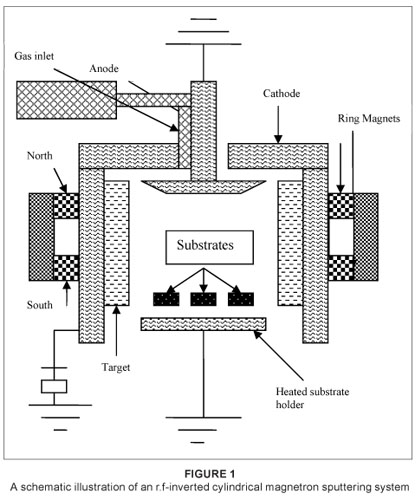
The films were deposited on soda lime glass substrates using r.f-inverted cylindrical magnetron sputtering (ICMS) from a vanadium target in an argon and oxygen atmosphere (Figure 1). This technique is defined as a supplementary exceptional way to engineer nano-systems at high deposition rates onto complex-shaped substrates. This system consists of a cylindrical ring vanadium metal target with a circular magnet enclosed behind the target. The ring magnets are there to enhance the electron path. Because the electron path is not on a straight line as a result of the magnetic field, the collision probability of an electron with ions is high and therefore the plasma is enhanced. The vacuum chamber was fitted with two gas inlets to introduce a mixture of argon and oxygen gases for reactive sputtering. The gas flow was controlled with a leak valve and the pressure inside the chamber was monitored by Penning and Pirani gauges. A Dressler Cesar RF power generator was used as a power supply. Prior to the deposition, the system was evacuated by a diffusion pump backed by a rotary pump down to 10-6 mbar. A mixture of argon and oxygen (argon was used as the working gas for enhancing plasma and oxygen as a reactive gas), was let into the sputter chamber. For all deposition processes, a mixture of argon (90%) and oxygen (10%) was introduced to the chamber at a pressure of 8x10⁻³ mbar followed by a high-purity argon (99.99%) flow at a pressure of 10-2 mbar. This gas composition and pressure were found to be optimal for getting thermochromic VO2. The deposition time and power were fixed at 2 h and 70 W, respectively, in all depositions. The deposition temperature ranged from 450 ºC to 550 ºC. The lowest deposition temperature to obtain crystalline VO2 was found to be 450 ºC.
SAMPLE CHARACTERISATION
The following sections describe the characterisation technique used and the conditions during experimentation.
X-ray diffraction technique
X-ray diffraction (XRD) is described as a powerful non-destructive technique for the characterisation of crystalline materials.9,10 It provides information on the structure, phase, preferred crystal orientation (texture) and other structural parameters, such as average grain size, strain and crystal defects.
When a monochromatic X-ray beam with wavelength λ, on the order of lattice spacing d, is projected onto a crystalline material at an angle θ, X-ray diffraction peaks are produced by constructive interference of the monochromatic beam scattered from each set of lattice planes at specific angles. Constructive interference gives the diffraction peaks according to Bragg's law,

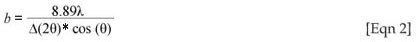
By varying the angle θ, the Bragg's law condition is satisfied by different d-spacings in polycrystalline materials. Plotting the angular position and intensities of the resultant diffracted peaks of radiation produces a pattern, which is characteristic of the material. The full width at half maximum of the peak, Δ (2θ) (in radians), is a measure of the grain size b in a polycrystalline film or the mosaic blocks in an epitaxial layer, as described by Scherrer's formula:
The XRD equipment that was used for this work is the Bragg-Brentano diffractometer, with Cu Kα (λ = 0.15418 nm) radiation and a scintillation detector. The X-ray tube was typically operated at a voltage of 40 kV and a current of 20 mA. One scan mode, θ – 2θ scan, was used for microstructural characterisation. The detector rotated twice as fast and in the same direction around the diffractometer axis as the sample. This technique is also called the locked-coupled scan. In the θ – 2θ scan, the reflections from the planes parallel to the substrate surface were detected. This allowed us to determine the orientation along the growth direction of the (epitaxial or polycrystalline) films with respect to the substrate.
UV-VIS spectrophotometry
The UV-VIS spectrophotometer that was used in this work consists of a light source, a sample holder fitted with a heating stage, a detector and a data acquisition computer.11,12 The sample holder is located between the light source and the detector. The light source, detector and sample holder are designed to fit within a dark box that has a cover to prevent unwanted light interfering with the laser beam during experimentation. The wavelength range of the spectrophotometer is 200 nm – 1100 nm. The spectrophotometer was allowed to create a baseline which removes background from the data to be collected. The beam of light is directed to the sample and the detector detects the amount of light transmitted through the sample.
The data was generated and captured by the computer and temperature measurements were recorded. The data collected was used to plot the graphs of transmittance as a function of wavelength. The UV-VIS spectra were used to investigate the optical switching property of the deposited VO2 films.
RESULTS AND DISCUSSION
Film microstructure
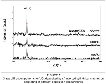
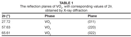
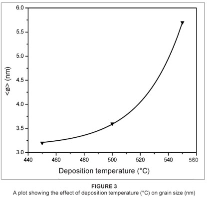
The XRD spectra (scanned from 20º to 70º) of the VO2 thin films deposited at different deposition temperatures are shown in Figure 2. The scan was taken at room temperature, in the semiconducting phase of VO2 (monoclinic structure). The films exhibit a polycrystalline structure whose peaks match the single phase of monoclinic VO2 (JCPDS 044-0225) without showing the indication of other VO2 phases. The reflection planes with their corresponding values of 2θ are given in Table 1. All the films show a first peak at the (011) plane, indicating the presence of VO2.6,13,14,15 The XRD spectra of the film deposited at a deposition temperature of 450 ºC shows Bragg reflection at 2θ = 27.72º, corresponding to (011) reflection of the VO2 monoclinic phase. The grains of the VO2 thin films deposited at 450 ºC are highly oriented with crystallographic (0hh) planes parallel to the substrate plane. The (011) reflection emerges from a broad structure. The broad structure may suggest the existence of a disordered phase of VO2. The XRD spectra of the film deposited at a deposition temperature of 500 ºC exhibited the same behaviour as that of the film deposited at 450 ºC. The film deposited at a deposition temperature of 550 ºC exhibited similar XRD patterns. In addition to the (011) peak, the patterns show the emergence of new peaks at 2θ = 57.63º and 65.61º corresponding to the (220) and (022) reflections, respectively. The appearance of new reflections is a clear indication of the deterioration of the orientation of the VO2 grains when the temperature increases. The peak at the (011) reflection was used to estimate the average grain size. The average grain size was estimated using Debye's formula:

The estimated values were then used to plot the graph shown in Figure 3. The graph was used to observe the influence of deposition temperature on the grain size of the VO2 thin film.
Thermochromism of the film
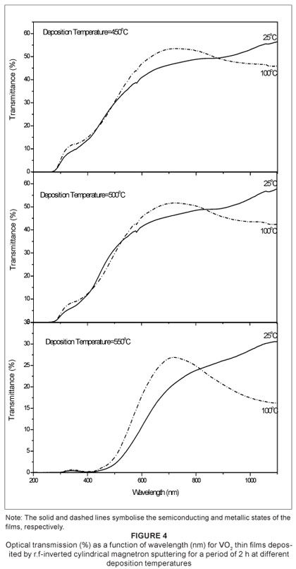
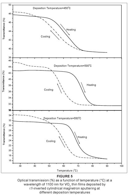
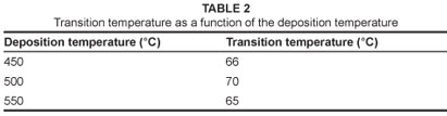
Figure 4 shows the film optical transmittance (%) as a function of wavelength (nm) of the VO2 thin films deposited by ICMS. The spectral transmittance observed at a low temperature (25 ºC) semiconducting phase and a high temperature (100 ºC) metal phase showed a sharp contrast in the infrared region. The metallic phase exceeds the semiconducting phase in the infrared region in all films, which indicates that the film is less than 100 nm as demonstrated by Xu et al.8 The highly oriented VO2 film obtained at 450 ºC exhibits higher transmission switching efficiency than the films obtained at 500 ºC and 550 ºC. Figure 5 show the hysteresis loops of transmittance as a function of temperature (at a fixed wavelength of 1100 nm) for the VO2 thin films. The hysteresis width of the films deposited at a deposition temperature of 450 ºC is approximately 5 ºC. The films obtained at 500 ºC and 550 ºC have the same hysteresis width of approximately 10 ºC. The transition temperatures are shown in Table 2. All the films have the same hysteresis sharpness. The transition temperature of the films slightly decreases when deposition temperature increases. It is suggested that this slight decrease is caused by the random arrangement of the grains in the film deposited at 550 ºC.
Electrical measurements of the film
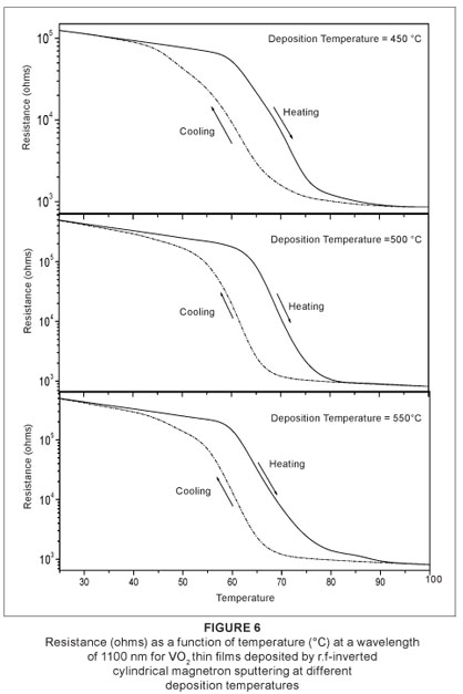
Figure 6 shows the resistance hysteresis loops of VO2 thin films deposited at temperatures of 450 ºC, 500 ºC and 550 ºC. The film deposited at 450 ºC exhibits a sharp transition in electrical resistance near 68 ºC, which is a definitive confirmation of formation of thermochromic VO2. The drop in the electrical resistance is about two orders of magnitude, which is similar to the one observed in high-quality polycrystalline VO2 thin films but less than that reported by Kucharczyk and Niklewski16 for a single bulk crystal of VO2. The temperature hysteresis width is approximately equal to 10 ºC. This large hysteresis of the VO2 film compared to that observed in a single bulk VO2 crystal (2 ºC), may have its origin in the extrinsic stress created during deposition by the difference in thermal expansion coefficients between the VO2 film and the substrate. The films deposited at 500 ºC and 550 ºC exhibit the same behaviour in terms of electrical switching. The transition is sluggish and shifts towards lower temperature near 66 ºC. The drop in the electrical resistance is about three orders of magnitude. Both films exhibit a temperature hysteresis width of about 10 ºC. The decrease in the sharpness of the transition profile and the magnitude of the drop in the electrical resistance is caused by the random arrangement of the grains in the film, leading to different grain boundaries. The increase in deposition temperature affected the microstructure of the film, which led to the decrease in electrical and optical properties.
CONCLUSION
VO2 thin films were successfully synthesised on soda lime glass substrates. An increase in deposition temperature gives rise to an increase in grain size and causes deterioration of the orientation (texture) of the grain. An increase in deposition temperature enhances the peak intensity. An increase in deposition temperature also results in decreases in the optical and electrical properties of the film. It is clear that the electrical and optical switching of VO2 thin films depends on the synthesis conditions of the technique.
ACKNOWLEDGEMENTS
The authors would like to thank the National Research Foundation, South Africa for funding the project.
REFERENCES
1. Chain EE. Preparation and characteristics of VO2 thin film micro-bolometer application. J Vac Sci Technol A. 1986;4:432. [ Links ]
2. Chain EE. Effects of oxygen in ion-beam sputter deposition of vanadium oxide. J Vac Sci Technol A. 1987;5:1836. [ Links ]
3. Case FC. Influence of ion beam parameters on the electrical and optical properties of ion-assisted reactively evaporated vanadium dioxide thin films. J Vac Sci Technol A. 1987;5:1762–1766. [ Links ]
4. Remka L, Walser RM, Bene RV. Optical switchable thin films. Thin Solid Films. 1979;61:73. [ Links ]
5. Bubert H, Jenett H. Surface and thin film analysis. Berlin: Wiley-VCH Verlag, 1992; p. 103–109. [ Links ]
6. Morin F. Oxides which show a metal-to-insulator transition at the Neel temperature. Phys Rev Lett. 1959;3:34. [ Links ]
7. De Waal HS. Compound phase formation at AU-A1 interfaces. New York: Addison-Wesley Publishing Company, 1995; p. 59–78. [ Links ]
8. Xu G, Jin P, Tazawa M, Yoshimura K. Thickness dependence of optical properties of VO2 thin films epitaxially grown on sapphire (0 0 0 1). Appl Surf Sci. 2005;244:449–452. [ Links ]
9. Warren BE. X-ray diffraction. New York: Addison-Wesley Publishing Company, 1969; p. 61–83. [ Links ]
10. Introduction to X-ray diffraction [homepage on the Internet]. No date [cited 2007 Aug 23]. Available from: http://www.panalytical.com/index.cfm?pid=135 [ Links ]
11. Introduction to spectrophotometry [homepage on the Internet]. No date [cited 2007 Aug 16]. Available from: http://www.varianinc.com.cn/products/spectr/uv/brochure/1604.pdf [ Links ]
12. Introduction to spectrophotometry [homepage on the Internet]. No date [cited 2007 Aug 22]. Available from: http://webche.ent.ohiou.edu/che416/UV_w02.html [ Links ]
13. Vernardou D, Manning TD, Parkin IP, et al. Intelligent window coatings: Atmospheric pressure chemical vapour deposition of tungsten-doped vanadium dioxide. Surf Coat Technol. 2004;188–189:250. [ Links ]
14. Maaza M, Bouziane K, Maritz J, et al. Direct production of thermochromic VO2 thin film coatings by pulsed laser ablation. Opt Mater. 2000;15:41–45. [ Links ]
15. Golan G, Axelevitch A, Sigalov B, Gorenstein B. Metal insulator phase transition in vanadium oxide films. Microelectr J. 2003;34:255–258. [ Links ]
16. Kucharczyk D, Niklewski T. Accurate X-ray determination of the lattice parameters and the thermal expansion coefficients of VO near the transition temperature. J Appl Crystallogr. 1979;12:370. [ Links ]
 Postal address:
Department of Mechanical Engineering, Cape Peninsula University of Technology
PO Box 1906
Bellville 7535, South Africa
Received: 31 July 2009
Accepted: 28 Sept. 2010
Published: 18 Nov. 2010
Correspondence to: Velaphi Msomi
This article is available at: http://www.sajs.co.za
© 2010. The Authors. Licensee: OpenJournals Publishing. This work is licensed under the Creative Commons Attribution License.

