


Services on Demand
Article
 English (pdf)
 Article in xml format
 Article references
Indicators

Related links
-
 Cited by Google
 -
 Similars in Google
Share

 Permalink
South African Journal of Science
On-line version ISSN 1996-7489
Print version ISSN 0038-2353
S. Afr. j. sci. vol.105 n.11-12 Pretoria Nov./Dec. 2009
RESEARCH ARTICLES
Solid-state compound phase formation of TiSi2 thin films under stress
C. TheronI; N. MokoenaII, III; O.M. NdwandweII, *
IDepartment of Physics, University of Pretoria, Pretoria 0002, South Africa
IIDepartment of Physics and Engineering, University of Zululand, Private Bag X1001, KwaDlangezwa 3886, South Africa
IIIReactor Fuel Engineering Group, Koeberg Nuclear Power Station, Private Bag x10, Kernkrag 7440, South Africa
ABSTRACT
Different stress situations were created on an Si(100) wafer by depositing either Si3N4 or SiO2 thin films on the back side. Si3N4 has a different thermal expansion coefficient from that of SiO2. A thin Ti film was then deposited on the front side of the Si wafer. The structures were then annealed at various high temperatures for different periods of time. Real-time Rutherford backscattering spectrometry, as well as sample curvature measurements, were used to characterise the samples. Different reaction rates were found between Si3N4-deposited samples and SiO2-deposited samples.
Key words: stress, thin films, real-time Rutherford backscattering spectrometry, phase formation, TiSi2, diffusion
Introduction
Stress is always present in thin films due to film deposition parameters. These parameters include the type of film that has been deposited, the rate of deposition, the method that was used to deposit the films, and the temperature of the substrate during deposition.1 According to Yu,2 stress in thin films may be divided into: thermal stress, due to the difference in thermal expansion coefficients of the film and the substrate; or intrinsic stress, which results from the growth and the structure of the films. For film thicknesses (tf) that are much smaller than substrate thicknesses (ts), Stoney's equation is generally used:1
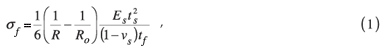
where Es is Young's modulus, νs is Poisson's ratio of the substrate, and R and Ro are the radii of curvature of the film before and after film deposition, respectively.
TiSi2 is of great technological importance to the microelectronics industry and has widespread use in the fabrication of metal oxide semiconductor field effect transistors (MOSFET).3 TiSi2 is a popular silicide because it has the lowest resistivity of all silicides.4,5 This fact has resulted in many studies being done on the reaction between Ti and Si thin films.6 Reports concerning first phase formation and phase formation sequence in the Ti-Si binary system vary. Some investigators have reported that TiSi2 is the only phase found at temperatures greater than 500°C.7 Other studies show that all the Ti is converted to TiSi, before the formation of TiSi2, at temperatures between 450°C and 700°C.8
Some investigators have performed rapid thermal annealing (RTA) studies and have found that TiSi first forms at temperatures between 450°C and 600°C.9 There are however other investigators who reported Ti5Si4 as a first phase during RTA studies.10 In some investigations, TiSi grew simultaneously with TiSi2, Ti5Si4 and Ti5Si3, at temperatures between 400°C and 600°C.11
Methods
Samples with the structures SiO2/Si<100> or Si3N4/Si<100>, were chemically cleaned following a simple sequence. The following procedure was used: Samples were dipped, in sequence, in methanol, acetone, trichloroethylene, acetone and methanol, and then rinsed in ionised water. Finally, the samples were etched in a 20% solution of hydrofluoric acid to remove any native oxide layer that may be present. The role of the back side substrates, SiO2 and Si3N4, was to induce stress of different types during annealing. The samples were loaded in an ultra-high vacuum system where Ti of various thicknesses was deposited on the front side of the substrates. The vacuum during deposition was better than 6 × 10⁻⁷ torr. As a precaution, the samples were kept in a vacuum overnight to allow them to cool. Ti is known to easily oxidise in air, especially if its temperature is elevated. The resulting structures, SiO2/Si<100>/Ti or Si3N4/Si<100>/Ti, were then annealed in a furnace at temperatures ranging from room temperature to 650°C. Ti was also deposited on Si<100> without a back side layer, under the same condition as the other samples.
In order to measure stress, sample thicknesses were accurately determined. First we used Rutherford backscattering spectrometry (RBS) in order to find layer thicknesses as well as to check whether the correct stoichiometry, in the case of back side SiO2 and Si3N4, had been obtained during sample preparation. A screw gauge was then used to determine wafer thickness.
Results and discussion
Rutherford backscattering spectrometry results for the front side of the wafer showed that the thickness of the Ti was 550 Å . The thickness of the wafer, measured by means of a screw gauge, was found to be 6 230 000 Å.
From the relationship expressing change in length (ΔL) with change in temperature (ΔT)

where L is the length of the film, we can express the ratio of the change in length of the film and the substrate in terms of expansion coefficients,

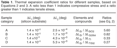
(since L1 ≈ L2). Results of such a calculation for the different sample categories in our experiment are summarised in Table 1. A ratio of less than one implies that a compressive stress will develop on the front side of the sample upon heating (a ratio bigger than one implies a tensile stress will develop).
Equation 410 was used to calculate the stress in the deposited film:
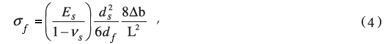
where

and Δb = b – b0, thus the bow is related to the experimental radius (R1), b is its value after deposition and b0 the value before deposition (Fig. 1).


The stress is calculated on the entire sample since it has a depth of focus in the substrate (σsi(z)). The stress depth is calculated using the following equation:
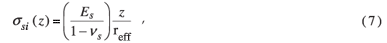
where z = 0 in the middle of the substrate and z = [1/2(623)] =311.5 at the front side deposited with Ti.
Stress was calculated using Stoney's equation, as given by Equation 1, and the value of R1 was determined from Equation 6. Radius measurements were obtained using a profilometer. This gave the length (L) and bow value (b) that was used to calculate radius R1. After the calculation of the sample radius (R1), Ro, the original radius before deposition of Ti, was obtained by using the radius effect.10 The two values, R1 and Ro, were then used to find the effective radius (Reff) of each sample. Reff allowed us to calculate the stress after deposition. Table 2 summarises the results of the calculation.
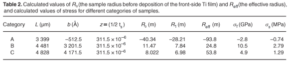
The negative sign on stress values indicate that the stress is compressive, while positive values indicate tensile stress. The stress is induced in the thin film when deposition takes place on the bare substrate. The sample heats up slightly during deposition and then cools after deposition is completed. When the film is being deposited on top of the substrate in a vacuum, by means of electron beam evaporation, it heats up due to the flux of energetic particles landing on the substrate and also because radiative heat is released from the molten material being deposited from the crucible. The composite film now has multilayers, which on cooling contract by unequal amounts due to different expansion coefficients of the different films. Thermal expansion coefficients of metallic films are generally larger in value when compared to those of silicon. But SiO2 has an even smaller expansion coefficient compared to that of Si. Si3N4 has a larger expansion coefficient compared to Si (Fig. 2 and Table 3).

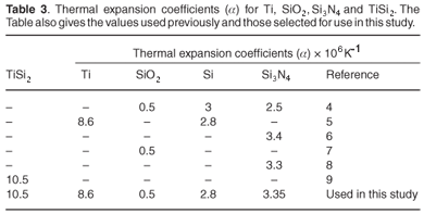
The front side film is therefore deposited at a temperature which is higher than room temperature because of the unintended heating effects explained before. When the sample cools down, the layer that has a higher expansion coefficient shrinks to a greater extent, causing either compressive stress or tensile stress on the front surface. In the case of a sample with structure SiO2/Si/Ti—if one neglects the effect of the Ti, since it is much thinner than the other two films—SiO2 will shrink less than Si, causing the front surface, and hence the Ti film, to be under compressive stress at room temperature. Si3N4 has a thermal expansion coefficient greater than that of Si. On cooling, Si3N4 will contract more than Si, leading to a tensile stress in the front of the film, where Ti is located (Fig. 2).
Normal Rutherford backscattering spectrometry
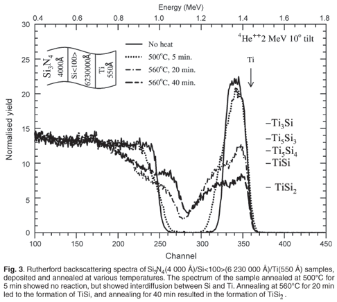
Figure 3 shows Rutherford backscattering spectra of a multilayered film made up of a Si<100> wafer onto which 4 000 Å of Si3N4 was deposited on the back side. The wafer itself is 6 230 000 Å thick. On the front side of the wafer, 550 Å of Ti was deposited. Rutherford backscattering spectrometry results showed no observable reaction for samples annealed at temperatures below 500°C (not shown here). The spectrum of the sample annealed at 500°C for 5 min showed interdiffusion between Ti and Si. This is indicated by the change in the gradient on the edge of the spectrum of Ti (that is in contact with Si), which changed from steep to less steep. No shoulder developed, indicating that no reaction took place. The spectrum of the sample annealed at 560°C for 20 min has a shoulder corresponding to the formation of TiSi. The formation of TiSi as a first phase in the Ti-Si thin films binary system has been observed previously by others.8 The presence of a compressive stress (at high temperature) on the front side of the wafer, due to Si3N4 on its back side, has therefore not led to any change in first phase formation for this binary system. The spectrum of the sample annealed at 560°C for 40 min showed the presence of TiSi2 (Fig. 3).
Samples comprised of SiO2(4 000 Å)/Si<100> (5 300 Å)/Ti(550 Å) were annealed at various temperatures. Figure 4 shows the spectra of a virgin sample and a sample annealed at 590°C for 40 min; it can be observed that TiSi formed on the annealed sample. Rutherford Universal Manipulation Program simulation showed that there was still Ti remaining on this sample after annealing. The sample was, however, already in an advanced state of reaction. It was not possible from the results obtained to determine at what exact temperature the reaction started on the samples with SiO2 on their back side. To solve this problem, we performed in situ real-time RBS.

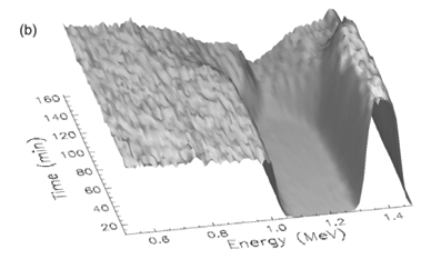
In situ real-time Rutherford backscattering spectrometry
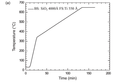
In order to observe when the reaction starts and how it proceeds with time, in situ annealing and spectrum collection from RBS were done simultaneously in a chamber whose vacuum was better than 10–6 torr. The heating was done by ramping the temperature, at a rate of 20°C min–1, from room temperature (~20°C) to 340°C. Thereafter, it was ramped at a rate of 3°C min–1 and allowed to rise to a value of 650°C. Figure 5a shows the temperature versus time curve as measured on the sample. Figures 5b and 5c show a three-dimensional view of the spectrum from a sample of a 6 230 000 Å thick Si<100> wafer with 4 000 Å of SiO2 deposited on the back side and 550 Å Ti on the front side. Figure 5b shows that there is no observable reaction between Si and Ti during the time period from 0 min to about 80 min (which corresponds to a temperature of about 500°C). A more in depth analysis of the spectra that make up Fig. 5 showed that TiSi began forming at that stage. It continued growing until about 110 min after starting the ramp. This time corresponds to a temperature of about 580°C. At that stage, TiSi2 formation was observed. These observations are in line with what was observed using normal RBS.

Annealing of the sample with Si3N4 on the back side was done by ramping the temperature, at a rate of 20°C min–1, from room temperature (~20°C) to 440°C. It was thereafter ramped at 3°C min–1, to 650°C. Rutherford backscattering spectrometry analysis on the sample with Si3N4, with a structure of Si3N4(400 Å)/Si (6 230 000 Å)Ti(400 Å), showed that the reaction for the formation of TiSi started at about 570°C, and formation of TiSi2 started at about 610°C. Both phases (TiSi and TiSi2) grew simultaneously thereafter with increasing temperature (RBS results not shown).
The RUMP simulation program was used to analyse the thicknesses of grown phases at different temperatures. Table 4 summarises the values of sample thicknesses observed.

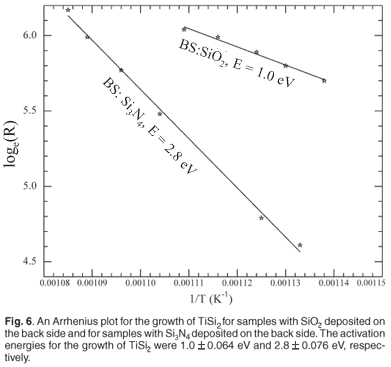
Figure 6 is an Arrhenius plot for the growth of the phase TiSi2, for the samples with SiO2 deposited on the back side and with Si3N4 deposited on the back side. The activation energy for the growth of TiSi2 in which the back side film was SiO2 was 1.0 ± 0.064 eV, and the activation energy for the growth of TiSi2 in which the back side film was Si3N4 was 2.8 ± 0.076 eV.
Conclusion
We investigated the interfacial reaction between Si and Ti by depositing either SiO2 or Si3N4 on the back side of a Si<100> wafer, so as to induce stress on the front side. Such stresses could be either compressive or tensile. A layer of Ti, which was much thinner than either the substrate Si or the back side layer, was then deposited on the front side of the wafer.
Characterisation of the samples, using RBS, after annealing in a vacuum at high temperatures revealed that TiSi formed first, followed by TiSi2. In situ real-time RBS allowed us to follow the process step-by-step and to more accurately determine the starting temperatures for phase formation. Real-time RBS showed that, for a sample with SiO2 on its back side, formation of TiSi started at 500°C, while TiSi2 began to form at 580°C. In the case of the sample with Si3N4, TiSi began forming at 570°C and TiSi2 at 610°C.
Activation energy for the formation of TiSi2 on the sample with a back side layer of SiO2, was found to be 1.0 ± 0.064 eV, while that for a sample with a back side layer of Si3N4, was found to be 2.8 ± 0.076 eV. Values of stress calculated at room temperature for a sample with SiO2 on its back side was found to be –2.8 GPa, while for a sample with Si3N4, it was 10.5 GPa.
It must be noted that in this experiment the annealing temperatures (>400°C) were much higher than the deposition temperatures (<100°C), which in turn were higher than the temperatures at which stress measurements were made. It was found that the sample with SiO2 on its back side displayed compressive stress on its front side at room temperature. When such a sample is annealed, the temperature-induced stress should reduce, reach a minimum at its deposition temperature and then rise again (but with an opposite sign) above the deposition temperature. This sample should therefore display tensile stress on its front side at the temperature at which phases form. Tensile stress causes the appearance of vacancies on the front side, thus leading to an easier diffusion of atoms (and hence a lower activation energy). The opposite should happen for a sample with Si3N4 on its back side.
1. Mayer J.W. and Lau S.S. (1990). Electronic Materials Science: for Integrated Circuits in Si and GaAs. Macmillan, New York. [ Links ]
2. Yu J.S., Mariaty A.M. and Knorr D.B. (1997). Model for predicting thermal stresses in thin polycrystalline films. J. Mech. Phys. Solids 45, 511–534. [ Links ]
3. La Via F., Privitera S., Grimaldi M.G., Rimini E., Quilici S. and Meinadi F. (2000). Determination of C54 nucleation site density in narrow stripes by sheet resistance measurements and µ-Raman spectroscopy. Microelectron. Eng. 50, 139. [ Links ]
4. Nicolet M.A. and Lau S.S. (1983). VLSI Electronics Microstructure Science, ed. N. Einspruck, p. 415. Academic Press, New York. [ Links ]
5. Grovenor C.R.M. (1989). Microelectronics Materials, p. 68. Adam Hilger, Bristol and Philadelphia. [ Links ]
6. Pretorius R., Theron C.C. and Marais T.K. (1993). Evaluation of anomalies during nickel and titanium silicide formation using the effective heat of formation model. Mater. Chem. Phys. 36, 31. [ Links ]
7. Beyers R. and Sinclair R. (1985). Metastable phase formation in titanium-silicon thin films. J. Appl. Phys. 57, 5240. [ Links ]
8. Pico C.A. and Legally M.G. (1988). Kinetics of titanium silicide formation on single crystal Si: Experiment and modeling. J. Appl. Phys. 64, 4957. [ Links ]
9. Wei C.S., van der Spiegel J. and Santiago J. (1985). Electrical characteristics of fast radiatively processed titanium silicide thin films. J. Vac. Sci. Technol. A 3, 2259. [ Links ]
10. Dexin C.X., Harrison H.B. and Reeves G.K. (1988). Titanium silicide formed by rapid thermal vacuum processing. J. Appl. Phys. 63, 2171. [ Links ]
11. Lakshmikumar S.T. and Rastogi A.C. (1989). The growth of titanium silicides in thin film Ti/Si structures. J. Vac. Technol. B 7, 604. [ Links ]
Received 23 October 2008.
Accepted 25 August 2009.
* Author for correspondence E-mail: muzi.ndwandwe@gmail.com

