


Serviços Personalizados
Artigo
 Inglês (pdf)
 Artigo em XML
 Referências do artigo
Indicadores

Links relacionados
-
 Citado por Google
 -
 Similares em Google
Compartilhar

 Permalink
South African Journal of Science
versão On-line ISSN 1996-7489
versão impressa ISSN 0038-2353
S. Afr. j. sci. vol.105 no.7-8 Pretoria Jul./Ago. 2009
RESEARCH LETTERS
Numerical solution of multiband k·p model for tunnelling in type-II heterostructures
A.E. Botha
Department of Physics, University of South Africa, P.O. Box 392, UNISA 0003, South Africa. E-mail: bothaae@unisa.ac.za
ABSTRACT
A new and very general method was developed for calculating the charge and spin-resolved electron tunnelling in type-II heterojunctions. Starting from a multiband k·p description of the bulk energy-band structure, a multiband k·p Riccati equation was derived. The reflection and transmission coefficients were obtained for each channel by integrating the Riccati equation over the entire heterostructure. Numerical instability was reduced through this method, in which the multichannel log-derivative of the envelope function matrix, rather than the envelope function itself, was propagated. As an example, a six-band k·p Hamiltonian was used to calculate the current-voltage characteristics of a 10-nm wide InAs/GaSb/InAs single quantum well device which exhibited negative differential resistance at room temperature. The calculated current as a function of applied (bias) voltage was found to be in semi-quantitative agreement with the experiment, a result which indicated that inelastic transport mechanisms do not contribute significantly to the valley currents measured in this particular device.
Key words: spin-dependent electron transport, semiconductor nanostructures
1. Introduction
Electron tunnelling phenomena associated with the broken-gap1 configuration in type-II semiconductor heterostructures have been studied both theoretically2 and experimentally.3 In these structures, the minimum in the conduction band of the material on one side of the hetero-interface lies at a lower energy than the maximum in the valence band of the material on the other side. Charge transfer between two adjacent layers can lead to the formation of a 2-D electron gas on one side and a 2-D hole gas on the other, even at zero bias. Interband tunnelling may thus occur between the spatially-separated intrinsic carriers situated on opposite sides of the hetero-interface, i.e. between electrons in the conduction band on one side and holes in the higher-lying valence bands on the other side.4 Under suitable conditions, electron-hole bound states (excitons) may be formed. The InAs/GaSb system, for example, is currently the most promising candidate for observing Bose-Einstein condensation of excitons.5
Since the electron states of both conduction and valence bands of the constituent semiconductors participate in the tunnelling process on an equal footing, theories of electron tunnelling in type-II heterostructures must include the band-mixing effects.6 Direct numerical solution of the multiband k·p Schrödinger equation, which is frequently employed to model these systems, is not feasible due to the inherent numerical instability that occurs in type-II systems. The numerical instability in these systems arises because of the simultaneous presence of propagating (real wave vector) and evanescent (imaginary wave vector) states. To circumvent the numerical difficulties that arise in such calculations, several innovative techniques have been proposed within the context of multiband k·p theory.7,8
Multiband formulations of the transfer matrix method (TMM) become numerically unstable in the simultaneous presence of evanescent and propagating states. For this reason the TMM is not very useful for studying type-II systems. In cases where the TMM fails, it is possible to propagate the scattering matrix instead.9 This technique was first applied to resonant tunnelling in GaAs/A1xGa1–xAs multilayer systems, with the influence of higher bands included.10 Although the scattering matrix method is numerically stable it is computationally no more efficient than the TMM. A third method, the multiband quantum transmitting boundary method,11 is slightly more efficient; although with modern processor speeds the time saved on a typical calculation may be minimal in practice.
In Section 2.1 of this article, a new and very general method is proposed for calculating the electronic structure and transport properties of type-II heterostructures. In common with the preceding methods, the theory is based on a realistic, multiband k·p envelope function description of the energy-band structure. Starting from the general form of the n×n matrix Schrödinger equation, a multiband k·p Riccati equation is derived for the logarithmic derivative of the envelope function matrix. In Section 2.2 a boundary condition is derived for the Riccati equation. This boundary condition is used to integrate the Riccati equation numerically over the entire heterostructure. In Section 2.3 it is shown how to obtain the reflection matrix R, which contains the tunnelling amplitudes for each of the n channels along its diagonal. In Section 2.4 it is shown how the solution to the Riccati equation may be incorporated into a self-consistent calculation of the confining potential profile. The current through a device may then be calculated according to the definition given in Section 2.5. In Section 3, the room temperature current was calculated as a function of applied voltage for a 10-nm wide InAs/GaSb/InAs quantum well device and the results were compared to an experiment.3 It was found that the calculated current-voltage characteristics were in semi-quantitative agreement with the measured characteristics. This agreement suggests that, contrary to previous claims, inelastic transport mechanisms did not play a significant role in the resonant interband coupling mechanism that was most likely responsible for the negative differential resistance.
2. Theory
2.1. Multiband k·p Riccati equation
Consider a heterostructure with its growth direction along the x-axis. In multiband k·p models the energy-band structure within each layer of the heterostructure is described by a set of coupled differential equations for the components of the slowly varying envelope function, Φ(x). It can be shown that the Schrödinger equation for the envelope function can be decomposed into the following very general matrix form:12
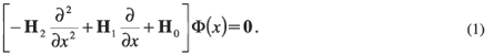
In Equation 1 the eigenvector Φ(x) is a column vector of length equal to the number of bands (n) which are explicitly included in the k·p model being used. The n × n matrices H0, H1 and H2 are usually derived through second order quasi-degenerate perturbation theory (Löwdin partitioning).13 Examples of the decomposition in Equation 1 can be found in Liu et al.,7 Harrison8 and Eppenga et al.14
Instead of working with an n-component column vector Φ(x), it is advantageous to construct an n × n envelope function matrix, denoted by F(x). This matrix contains in its columns the n, linearly independent solution vectors of the stationary problem posed by Equation 1.
It can be shown quite generally that H2 is non-singular.15 Equation 1 can therefore be multiplied throughout by  , resulting in

By substituting the general relation
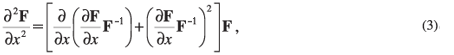
(which holds for any non-singular matrix F) into the left-hand side of Equaion 2, the multiband k·p Riccati equation

is obtained. Here Y has been defined as

In recognition of the logarithmic derivative form of Equation 5, Y will be referred to as the log-derivative of F.
2.2. Boundary condition for the Riccati equation
Consider the multiband potential profile of the heterostructure shown schematically in Fig. 1. The device consists of a central active region sandwiched between two flat-band contact regions. Assume that within the active region (xL, xR) the potential may vary arbitrarily, but that it remains constant (not necessarily zero) in the outer two contact regions, i.e. for x < xL and x > xR. By making the very reasonable assumption that all charge carriers are incident from the left contact region, it follows that there can be no reflected waves in the right contact region. For (x > xR), the matrix solution to Equation 1 can therefore be written in terms of transmitted plane waves as
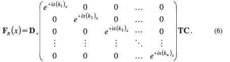
Here D+, T and C are n × n matrices. D+ is a known matrix whose columns are made up of the n linearly-independent eigenvectors of Equation 1 within the right contact region. Although D+ can be obtained analytically for relatively small values of n (for example, see Botha4), a more general numerical method has recently been suggested by Harrison.8 The numerical method consists of re-writing the non-linear eigenproblem posed by Equation 1 as a linear eigenproblem for the wave vector components (ki)x (i = 1, 2,..., n) (see Equation 10.35 in Harrison8). In Equation 6, T is an (as yet) unknown transmission matrix which depends only on the electron energy E, the transverse component of the carrier wave vector k|| and the applied voltage Va. The matrix C is constant with respect to x and may be chosen arbitrarily. It is most convenient to choose C such that FR(x0) = 1, where 1 is the n × n identity matrix and x0 > xR. By making this choice, and evaluating Equation 6 at x = x0, it follows that
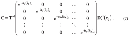
Because the wave vector components (ki)x and matrices D± only depend on x indirectly through the potentials Vi(x), D± can be treated as constants within the two contact regions. Equation 6 can therefore be differentiated partially with respect to x, yielding
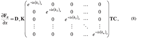
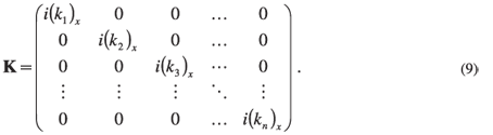
where
Evaluation of Equation 8 at x = x0, with C given by Equation 7, produces the result

Since FR(x0)= (x0)=1 (by choice of C), the boundary condition required to integrate Equation 4 is then clearly given by
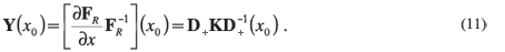
The main advantage of working with Y, as opposed to F, is that its entries never grow excessively large or small. Equation 4 can therefore be integrated without difficulty over several hundreds of nanometres, even in the presence of strong k·p coupling.
Once Y has been obtained by numerical integration of Equation 4 over the entire heterostructure, the tunnelling probabilities for each channel can be obtained from the reflection matrix R, defined next.
2.3. Reflection matrix
In the left contact region (see Fig. 1), for x < xL, the solution to Equation 2 can also be expressed in terms of plane waves. In this region there are both incident and reflected waves and the solution must be written as
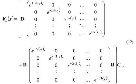
where D± are defined as before and R is the desired reflection matrix. By evaluating Equation 12 and its first derivative at x = 0, and multiplying both the resulting equations from the right by C–1, it is found that

and

Here K is defined as in Equation 9. Multiplication of Equation 14 from the right by the inverse of Equation 13, produces

By solving for R in Equation 15, the reflection matrix is obtained as

All quantities on the right of Equation 16 are to be evaluated at x = 0. The matrix Y(0) is obtained by integrating Equation 4 from some point x = x0 > xR back to x = 0, starting with the boundary condition given by Equation 11. Note that the diagonal entries in R contain the reflection amplitudes for each channel. It can be shown that transmission coefficient Ti for the ith channel is related to R by Ti = 1 –  (no sum over i), where Rii is the ith diagonal entry of R and
  denotes complex conjugation.
2.4. Self-consistent Schrödinger-Poisson scheme
Because the above method produces the log-derivative Y(x) it can be used to perform a fully self-consistent calculation of the heterostructure energy-band profile. This is an important advantage over other methods, such as the scattering matrix method which only produces the amplitudes of the envelope functions, not the functions themselves. Once Equation 4 has been integrated and Y(x) is known throughout the entire heterostructure, a second integration can be performed to obtain the envelope function matrix F(x) from Equation 5 and the boundary condition F(x0) = 1. By using the envelope functions, the energy-band profile and the corresponding reflection matrix can then be calculated self-consistently in conjunction with Poisson's equation.16
2.5. Current-voltage characteristics
Having obtained the transmission coefficients Ti as functions of the electron energy E, transverse component of the wave vector k|| and applied voltage Va; the current I flowing through the device can be calculated as a function of Va. For the InAs/GaSb/InAs quantum well device studied in Section 3, there is only one open channel and the current I flowing through the structure is defined as17,18
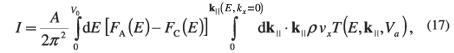
where FA and FC are the respective Fermi distribution functions for the left (anode) and right (cathode) contact regions. In Equation 17, A is the device area, T is the transmission coefficient, ρ is the density of states and νx is the incident carrier velocity. The latter two quantities are computed numerically by using the appropriate bulk carrier energy-dispersion relation.
3. Results
In this Section the above theoretical results are implemented numerically by using a six-band matrix Hamiltonian.19–21 In this model the basis has been chosen in order to decouple the spin components of the electron for kz = 0. Each of the two possible spin states of the electron can then be treated separately in terms of two identical 3×3 matrix Hamiltonians. For details concerning this model, including the k·p parameter values for InAs and GaSb, see Botha.4
There are a variety of numerical methods available for integrating coupled systems of first order differential equations such as Equation 4. Although the log-derivative form of Equation 4 is much simpler to integrate than the envelope function appearing in Equation 1, the integration subroutine nevertheless has to be quite sophisticated to take into account the discontinuities in the material parameters and potential as the integration proceeds through the heterostructure.22 The computations in this Section make use of an excellent integration subroutine called ODE. This subroutine is freely available and is described fully by Shampine and Gordan.23
The current I as a function of applied voltage Va has been computed for an InAs/GaSb/InAs quantum well device in which the GaSb layer is 10 nm wide. This device has been manufactured and studied experimentally.3 Based on the description of the device, the potential profile was calculated according to the self-consistent method outlined in Section 2.4. Figure 2 shows the calculated potential profile under zero bias and for Va = 0.6 V, respectively. In order to compute I, as defined in Equation 17, the calculated potential profile was used to obtain the corresponding transmission coefficient T according to the method described at the end of Section 2.3. Note that T is in general a function of the electron energy E, the perpendicular component of the wave vector ky (a good quantum number) and the applied voltage Va. As an example, the transmission spectrum is shown in Fig. 3 for ky = 0 and various applied voltage. The transmission spectrum differs considerably from that predicted by a simple two-band model in which the potential varies linearly.24 Instead of one broad resonance peak, corresponding to a confined light-hole resonant state in the GaSb layer, two narrower peaks are observed in Fig. 3. Physically, this more complicated transmission spectrum is the result of the coupling between a confined light-hole state in GaSb and quasi-bound electron states in the InAs anode. For ky ≠ 0 the transmission spectrum is further complicated by coupling of heavy-hole confined states in GaSb with quasi-bound electron states in InAs.
It is important to note that, in Fig. 2, for zero applied voltage there are two triangular quantum wells formed in the InAs layers which surround the GsSb barrier. As the applied voltage increases the potential profile gradually changes so that the triangular quantum well to the right of the barrier eventually disappears completely, as shown in Fig. 2 for Va = 0.6 V. On the other hand, an increase in applied voltage tends to increase the depth of the left triangular quantum well (in the anode). Coupling between the quasi-bound electron states in the InAs anode and the confined hole states in GaSb is responsible for the observed negative differential resistance. This coupling also accounts for the reduction in transmission peak height with increasing applied voltage, as seen in Fig. 3.
The transmission spectrum, calculated as in Fig. 3, produces the correct current-voltage behaviour for the device. Figure 4 shows the calculated room-temperature current through the device as a function of applied voltage. In this figure the calculated peak height has been normalised (using a multiplicative factor of 1.23) to the experimental peak height in the forward biased direction. This normalisation factor is required mainly because of the uncertainty in the device area (which is in the range of 10–5–10–4 cm2). In addition, there may be inevitable impurities in the sample and the value of the valence band offset between the two materials, and the position of the Fermi levels may also be uncertain.
The discrepancies between the current predicted by the present model and the much simpler two-band model, which was originally used to interpret the experimental data, do not alter the main conclusion which may be drawn from this experiment, namely that a resonant interband coupling mechanism is responsible for the observed negative differential resistance.3 However, unlike the two-band current-voltage model, the present model provides semi-quantitative predictions of the peak-to-valley ratios. Since the present model does not take into account inelastic transport mechanisms, it may be concluded from the agreement reached in Fig. 3, that contrary to what was previously thought, inelastic transport mechanisms do not contribute significantly to the observed valley currents in this device, even at room temperature. Whether this conclusion generalises to other similar structures depends on how well the model compares to the other available experimental data (for example see Collins et al.25). A more detailed investigation of the negative differential transport mechanism in GaSb/InAs heterostructures is currently in progress.
Finally, it should be emphasised that the preliminary results presented in this section are merely an example of how the general theory may be implemented and compared directly to an experiment. In this article, the main aim was to communicate the very general method that was developed in Sections 2.1–2.4. Since this method was based on the well-established multiband k·p model, it will be useful for theoretical studies of a wide variety of other interesting phenomena which occur in semiconductor heterostructures, for example, anisotropy (band warping)26 and spin-splitting (bulk, structural and due to an applied magnetic field).27
4. Conclusion
An alternative method was developed and implemented numerically to calculate electronic transport properties of type-II heterostructures. As an example, a realistic numerical implementation of the method was made by using a six-band matrix Hamiltonian in which the electron spin components decoupled. The preliminary results from this model have been compared to measured current-voltage characteristics of an InAs/GaSb/InAs quantum well device in which the GaSb layer width is 10 nm. The calculated current as a function of applied voltage was found to be in semi-quantitative agreement with the experiment3 and it was therefore concluded that inelastic transport mechanisms probably did not play a significant role in the device.
Given that only the bulk k·p parameters for the relatively simple six-band model were used in these calculations, the semi-quantitative agreement obtained from this model is encouraging and warrants further investigation. Such an investigation is in progress. The minor discrepancies between the model and experiment considered, in particular the necessity of using a current normalisation factor, can be attributed mainly to the uncertainty in the device area and the value of the valence band offset parameter.
1. Zakharova A. and Chao K.A. (2002). Influence of band state mixing on interband magnetotunnelling in broken-gap heterostructures. J. Phys.: Condens. Matter 14, 5003–5016. [ Links ]
2. Edwards G. and Inkson J.C. (1994). A microscopic calculation for hole tunnelling in type-II InAs/GaSb structures. Semicond. Sci. Technol. 9, 178–184. [ Links ]
3. Luo L.F., Beresford R., Longenbach K.F. and Wang W.I. (1990). Resonant interband coupling in single-barrier heterostructures of InAs/GaSb/InAs and GaSb/InAs/GaSb. J. Appl. Phys. 68, 2854–2857. [ Links ]
4. Botha A.E. (2006). Effect of remote band coupling on net recombination current in type-II heterostructures. Int. J. Nanosci. 5, 119–129. [ Links ]
5. De-Leon S. and Laikhtman B. (2000). Excitonic wave function binding energy and lifetime in InAs/GaSb coupled quantum wells. Phys. Rev. B. 61, 2874–2887. [ Links ]
6. Beresford R. (2007). Conserved flux in interband tunnelling. Solid State Electronics 51, 136–141. [ Links ]
7. Liu Y.X., Ting D.Z-Y. and McGill T.C. (1996). Efficient, numerically stable multiband k·p treatment of quantum transport in semiconductor heterostructures. Phys. Rev. B 54, 5675–5683. [ Links ]
8. Harrison P. (2005). Quantum Wells, Wires and Dots, 2nd edn., pp. 345–369. Wiley, New York. [ Links ]
9. Ikoni Z., Srivastava G.P. and Inkson J.C. (1992). Ordering of lowest conduction-band states in (GaAs)n/(AlAs)m [111] superlattices. Phys. Rev. B 46, 15150–15155. [ Links ]
10. Yu Kei Ko D. and Inkson J.C. (1988). Matrix method for tunnelling in heterostructures: resonant tunnelling in multilayer systems. Phys. Rev. B 38, 9945–9951. [ Links ]
11. Ting D.Z-Y. (1999). Multiband and multidimensional quantum transport. Microelectronics Journal 30, 985–1000. [ Links ]
12. Odermatt S., Luisier M. and Witzigmann B. (2005). Band structure calculation using the k·p method for arbitrary potentials with open boundary conditions. J. Appl. Phys. 97, 046104. [ Links ]
13. Winkler R. (2003). Spin-Orbit Coupling Effects in Two-dimensional Electron and Hole Systems, pp. 201–205. Springer, Berlin. [ Links ]
14. Eppenga R., Schuurmans M.F.H. and Colak S. (1987). New k·p theory for GaAs/Ga1–xAlxAs-type quantum wells. Phys. Rev. B 36, 1554–1564. [ Links ]
15. Smith D.L. and Mailhiot C. (1986). k·p theory of semiconductor superlattice electron structure I. Formal results. Phys. Rev. B 33, 8345–8359. [ Links ]
16. Tsu R. (2005). Superlattice to Nanoelectronics, pp. 100–103. Elsevier, Oxford. [ Links ]
17. Duke C.B. (1969). Solid State Physics: Advances in Research and Applications, suppl. 10, pp. 124–126. Academic Press, New York. [ Links ]
18. Liu Y.X., Marquardt R.R., Ting D.Z-Y. and McGill T.C. (1997). Magnetotunneling in interband tunnel structures.. Phys. Rev. B 55, 7073–7077. [ Links ]
19. Altarelli M. (1983). Electronic structure and semiconductor-semimetal transition in InAs-GaSb superlattices. Phys. Rev. B 28, 842–845. [ Links ]
20. Altarelli M. (1983). Electronic structure of semiconductor superlattices. Physica 117B & 118B, 747–749. [ Links ]
21. Altarelli M. (1983). Electronic structure of semiconductor superlattices. In Applications of High Magnetic Fields in Semiconductor Physics, ed. G. Landwehr, pp. 174–184. Springer, Berlin. [ Links ]
22. Johnson B.R. (1973). The multichannel log-derivative method for scattering calculations. J. Comp. Phys. 13, 445–449. [ Links ]
23. Shampine L.F. and Gordan M.K. (1975). Computer Solution to Ordinary Differential Equations: The Initial Value Problem. W.H. Freeman and Company, San Francisco. [ Links ]
24. Yu E.T., Collins D.A., Ting D.Z-Y., Chow D.H. and McGill T.C. (1990). Demonstration of resonant transmission in InAs/GaSb/InAs interband tunnelling devices. Appl. Phys. Lett. 57, 2675–2677. [ Links ]
25. Collins D.A., Yu E.T., Rajakarunanayake Y., Söderström J.R., Ting D.Z-Y., Chow D.H. and McGill T.C. (1990). Experimental observation of negative differential resistance from InAs/GaSb interface. Appl. Phys. Lett. 57, 683–685. [ Links ]
26. Botha A.E. and Singh M.R. (2002). The effect of anisotropy on resonant tunnelling spin polarization in type-II heterostructures. Phys. Stat. Sol. (b) 231, 437–445. [ Links ]
27. Pfeffer P. and Zawadzki W. (1999). Spin splitting of conduction subbands in III–V heterostructures due to inversion asymmetry. Phys. Rev. B 59, R5312–R5315. [ Links ]
Received 18 May. Accepted 5 June 2009.

