


Serviços Personalizados
Artigo
 Inglês (pdf)
 Artigo em XML
 Referências do artigo
Indicadores

Links relacionados
-
 Citado por Google
 -
 Similares em Google
Compartilhar

 Permalink
South African Journal of Science
versão On-line ISSN 1996-7489
versão impressa ISSN 0038-2353
S. Afr. j. sci. vol.105 no.7-8 Pretoria Jul./Ago. 2009
RESEARCH LETTERS
Synthesis of nanocrystalline silicon thin films using the increase of the deposition pressure in the hot-wire chemical vapour deposition technique
S. HalindintwaliI, *; D. KnoesenI; R. SwanepoelI; B.A. JuliesI; C. ArendseI; T. MullerI; C.C.TheronII; A. GordijnIII; P.C.P. BronsveldIII; J.K. RathIII; R.E.I. SchroppIII
IPhysics Department, University of the Western Cape, Private Bag X17, Bellville 7535, South Africa
IIMaterials Research Group, iThemba LABS, P.O. Box 722, Somerset West 7129, South Africa
IIISID – Physics of Devices, Utrecht University, P.O. Box 80.000, 3508 TA Utrecht, the Netherlands
ABSTRACT
Nanostructured thin silicon-based films have been deposited using the hot-wire chemical vapour deposition (HWCVD) technique at the University of the Western Cape. A variety of techniques including optical and infrared spectroscopy, Raman scattering spectroscopy, X-rays diffraction (XRD) and transmission electron microscopy (TEM) have been used for characterisation of the films. The electrical measurements show that the films have good values of photoresponse, and the photocurrent remains stable after several hours of light soaking. This contribution will discuss the characteristics of the hydrogenated nanocrystalline silicon thin films deposited using increased process chamber pressure at a fixed hydrogen dilution ratio in monosilane gas.
Key words: hot-wire deposition, intrinsic, absorption coefficient, degradation measurements, stability, photoresponse
Introduction
Hot-wire chemical vapour deposition, also known as catalytic chemical vapour deposition, is one of the techniques used to prepare thin amorphous and microcrystalline films for photovoltaic and large-area electronic applications.1–4 The process involves the catalytic decomposition of the feed gases over a resistively heated filament followed by a deposition of a layer on a substrate kept in an evacuated chamber. When silane or a silane/hydrogen mixture are used as feed gases, films ranging from amorphous to polycrystalline hydrogenated silicon can be obtained by proper control of the deposition parameters such as the hydrogen dilution ratio in the silane gas,5 the substrate and filament temperature4,6 and the process pressure. Hydrogenated nanocrystalline silicon (nc-Si:H)-based devices have been reported to be more stable than their amorphous (a-Si:H) counterparts.7 Klein et al.8 have recently shown that microcrystalline silicon films grown at a high deposition rate could be obtained at a high deposition pressure, but the material quality decreased. In this study, good-quality intrinsic nanocrystalline silicon films have been deposited using the increase of the deposition pressure at deposition rates as high as 4.7 s–1.
Methods
Thin films ranging from ~500 nm to 1 000 nm were deposited onto 2 cm × 2 cm Corning glass and c-Si (100) substrates. More details on the deposition chamber and the deposition process have been given elsewhere.9,10 The thickness was calculated using the computing method of Swanepoel11 and measured by a Dektak profilometer. For this effect, a Veeco Dektak 6M profiler was used to take measurements electromechanically by moving the sample beneath a diamond-tipped stylus that rides over the sample surface. The scan traces were always taken from a bare area of the substrate to the surface of the deposited layer and average step heights were calculated to estimate the thickness using the interfaced software.12 To ensure that the films were free of impurities during growth, a background pressure of less than 10–7 mbar was always achieved before deposition. The tantalum filament catalyser consisted of seven parallel wires maintained at 1 600°C. The temperatures of the substrate heater (Tsub.) were preset at 375°C, 410°C and 450°C. The distance between the filament and the substrate was fixed at 3.6 cm. Table 1 gives the details of the deposition conditions of the films used in this paper. The hydrogen dilution ratio in the silane gas was calculated as

where øH2 and øSiH4 represent the flow rates of hydrogen and silane, respectively. The phase changes were observed by XRD and by Raman scattering spectroscopy. X-ray diffraction spectra were obtained by means of a D8 advance Bruker diffractometer, a theta-2 theta (θ-2θ) machine situated at iThemba LABS, Faure. The used X-ray radiation was Cu Kα, with a wavelength of 0.15 nm. The intensity of the diffracted radiation was detected as a function of 2θ. In this study the value of 2θ varied from 22° to 70.72° with an angular resolution of 0.04° and an accumulation time of 30 s per step, i.e. 10 h per sample. Raman measurements were performed using the 514.5 nm line of a Spectra Physics Ar+-ion laser, a SPEX triple-grating monochromator and a CCD-detector situated in the Physics Department, Utrecht University (the Netherlands). The crystalline volume fractions (fc) were calculated from the deconvoluted peaks using the Raman data according to

where Ic, Igb and Ia are the integrated intensities of the crystalline peak, intermediate peak of the amorphous to crystalline phase, and the amorphous phase respectively.13 The hydrogen content (CH) was calculated from Fourier transform infrared spectroscopy measurements, using the integrated absorption coefficient of the rocking mode vibration at ~640 cm–1.ref. 14 For dark conductivity and photoconductivity measurements, two silver electrodes with a length of 20 mm separated by a distance of 0.5 mm were deposited on the samples. The photoconductivity was measured using a solar simulator with the AM1.5 spectrum at an intensity of 100 mW cm–2 ref. 15 and an applied voltage of 100 V. For activation energy (Ea) measurements, dark currents were measured from films successively annealed and cooled down in a vacuum from 160°C to room temperature. Activation energy was obtained from the Arrhenius plot of the dark conductivity data versus the reciprocal temperature in the cooling region. The light degradation experiment was done using the same setup as the one used by Britton et al.16 The samples were illuminated for 300 h and the photocurrent was measured at different time intervals at an applied voltage of 50 V.

Results and discussion
Phase transition
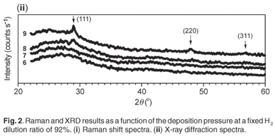
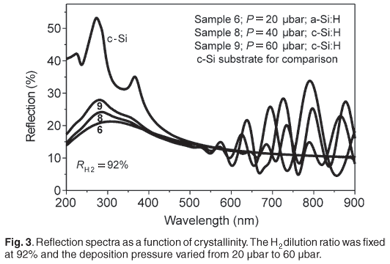
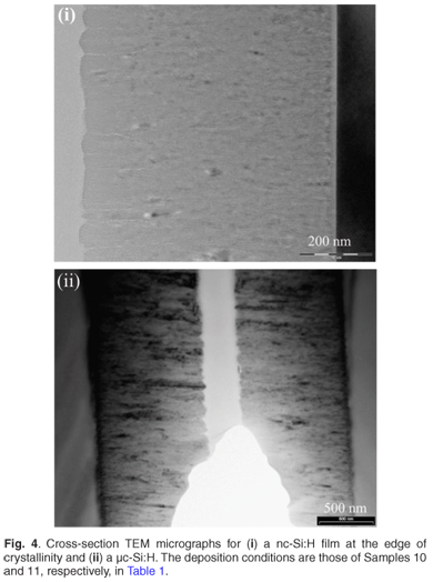
Figure 1 displays the Raman spectra of the films deposited at a fixed hydrogen dilution ratio of 87% with the deposition pressure varying from 20 µbar to 60 µbar. The first three samples deposited within the range 20–40 µbar were fully amorphous, as shown by the broad peaks centred around 480 cm–1. The fourth sample deposited at a pressure of 60 µbar was just above the edge of crystallinity. Its Raman spectrum is showing an asymmetry towards 520 cm–1 and its deconvolution into different Gaussians produced a small peak around 506 cm–1 in addition to the amorphous one centred around 480 cm–1. This has been interpreted as the inclusion of a finite number of small crystallites in an amorphous network. A crystalline volume fraction equal to 6% was calculated for this sample. The abundance of atomic hydrogen on, or near, the growing surface is essential for a change from an amorphous phase to a crystalline phase4,17 as the atomic hydrogen is known to passivate the surface and to etch away weak Si-Si bonds in the subsurface region.18 An increase of the deposition pressure had the beneficial effect of increasing the silane conversion rate and thus generating more silicon and atomic hydrogen precursors. It was even easier to induce crystallinity by increasing the pressure within the same range of 20–60 µbar at a fixed higher hydrogen dilution of 92% as shown in Fig. 2;19 increasing values of hydrogen dilution ratio produced more atomic hydrogen resulting from an increased splitting of molecular hydrogen on the hot filament. In Fig. 2(i), an increasing trend of the peak centred around 515 cm–1 with an increase in pressure, is observed on the spectra corresponding to Samples 7–9. The increasing Raman intensity of this peak at increasing process pressure is indicating an increase of the crystalline volume fraction. Sample 6 remains amorphous as its Raman spectrum shows only a broad peak centred around 480 cm–1. The XRD results in Fig. 2(ii) agreed well with the Raman results for Samples 6, 8 and 9. The XRD spectrum of Sample 7 was not conclusive enough, suggesting that, for films near the edge of crystallinity, a complementary sensitive method must be used to confirm the phase of the material. The UV-VIS reflection measurements on the same samples in Fig. 3 agreed with the XRD and Raman findings for the three investigated films (Samples 6, 8 and 9); the crystal Si direct-transition UV reflectance signatures at 365 nm and 275 nm20 revealed the presence of any crystalline phase at the surface. No crystalline signature was observed in the case of Sample 6, meaning that it was fully amorphous. The transition peaks for Samples 8 and 9 are distinguishable around 275 nm; they are not sharp as in the case of the c-Si substrate due to the residual amorphous network. Figure 4 displays the typical cross-section transmission electron micrographs of a nc-Si:H film near the edge of crystallinity with a crystalline volume fraction of 8% and a µc-Si:H film with fc of 53%. They are identified as Samples 10 and 11 in Table 1. The dark regions dispersed in much brighter areas are the crystals embedded in an amorphous network. The crystal sizes observed from TEM fell in the calculated range of about 2–40 nm as determined by the Scherrer formula on XRD data.


Deposition rate
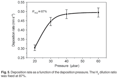
Figure 5 shows the deposition rate against the deposition pressure at a fixed hydrogen dilution ratio of 87%; it is observed that the deposition rate increased with an increase in pressure until a point where it saturated. The supply of Si-containing radicals increased with the process pressure; but since the surface of the filament was limited, a saturation point of the decomposition of the feed gas would have been reached and thus the deposition rate saturated. For the films deposited at a higher hydrogen dilution of 92%, at increasing chamber pressures within the same range of 20–60 µbar, slower growth rates were observed (2.17–3.00 Å s–1). This is explained by both the depletion of the SiH4 gas in the chamber resulting in less species decomposed on the filament for film growth, and the increase of H2 in the chamber giving rise to the concentration of atomic hydrogen decomposed from the filament that, in turn, increased the etching effect on the growing surface.21
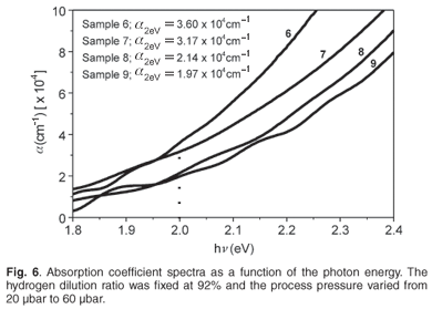
Absorption coefficient
Figure 6 shows the absorption coefficient (a) spectra for films ranging from amorphous to microcrystalline silicon. They were processed using the deposition conditions of Samples 6–9 as given in Table 1. As expected, the amorphous sample deposited with a deposition pressure of 20 µbar had higher α-values in the visible part of the spectrum than the microcrystalline films. Its value at 2 eV (~600 nm) was greater than the minimum reference value of 3.5 × 104 cm–1 for 'device quality' amorphous silicon films.22 Furthermore the calculated values for the three µc-Si:H films all had, at the same wavelength of the spectrum, relatively high values (greater than 1 × 104 cm–1) decreasing with the increase in crystallinity. This improved light absorption of the two-phased material was attributed to the remaining amorphous network in the films, which allowed direct optical transitions.
Electrical properties
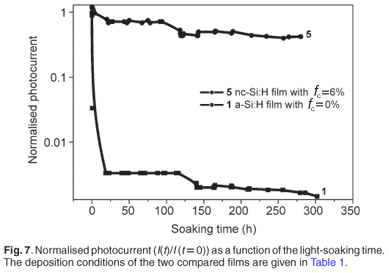
Table 2 summarises the electrical characteristics of Samples 2–5. It transpired from the table that the dark conductivity values were low, a sign that the films were truly intrinsic and the incorporation of impurities had been minimised. They compared well with the reported value for an amorphous silicon 'device quality' film of <1 × 10⁻¹⁰ Ω–1 cm–1.ref. 22 The values recorded for the activation energy supported this observation, as they agreed with the calculated energy gap values found in the range ~1.6–1.9 eV. The photoresponse of Sample 5 was maintained particularly high for a film above the edge of crystallinity, showing that the carriers recombination on the grain boundaries was insignificant. We conclude that the film contained a sufficient amount of hydrogen, as depicted in the last column of Table 2, such that the grain boundaries were passivated very well. A degradation study was conducted on the sample to investigate its stability under illumination. Figure 79 displays the measured photocurrent values as a function of the light-soaking time. The stability of Sample 5 (Table 1) was high as the change in photocurrent after more than 200 h of illumination was observed to be far less than one order of magnitude. The measured small value of the dark current was not affected by the illumination, and thus maintained the photoresponse at a high level. Compared to the graph of an amorphous Si film identified as Sample 1 in Table 1, it follows that the nanocrystalline material showed an improved stability against light exposure. This result is in agreement with other published reports.23 The noticeable difference between our results and those reported by Souffi et al.23 is the sharper drop of the photoconductivity for our amorphous film in the first 20 h of illumination. On the other hand, the photocurrent of the two films probed in our investigation stabilised after 200 h of illumination. The last observation was one of the advantages of a-Si:H films deposited by HWCVD over those deposited by plasma-enhanced chemical vapour deposition (PECVD).

Those deposited by PECVD reportedly do not attain a stable photoconductivity after several hours of illumination,24 in contrast to the HWCVD samples investigated in this study.
Conclusion
An increase in the deposition pressure at a fixed optimum hydrogen dilution ratio in the HWCVD process can be used to produce nc-Si:H intrinsic films that are both photosensitive and stable against light degradation effects. It has been shown that at a fixed relatively low hydrogen dilution ratio of 87% in silane, the films remained amorphous up to 60 µbar. When the hydrogen dilution ratio was increased to 92%, a gradual increase of the process pressure allowed the crystallisation of the films at a much lower pressure of 30 µbar. This method of inducing crystallinity using an increase in deposition pressure is particularly beneficial because relatively high deposition rates are achieved, although a saturation point will ultimately be reached due to the limited surface area of the filament catalyser. In this study, a deposition rate as high as 4.7 Å s–1 was achieved for a film at the edge of crystallinity with a crystalline volume fraction of 6%. The electrical properties studies have shown that this layer has a good photoresponse of 6.08 × 10³ while the degradation measurements have shown that the sample is quite stable.
The research described in this paper was financially supported by the National Research Foundation of South Africa (GUN 2050646). S.H. wishes to thank Utrecht University for the Werner van der Weg fellowship grant. iThemba LABS and the University of Cape Town are acknowledged for XRD and degradation measurements, respectively.
1. Wiesmann H., Gosh A.K., McMahon T. and Strongin M. (1979). a-Si:H produced by high-temperature thermal decomposition of silane. J. Appl. Phys. 50, 3752–3754. [ Links ]
2. Matsumura H. (1986). Catalytic chemical vapor deposition (CTL-CVD) method producing high quality hydrogenated amorphous silicon. Jpn. J. Appl. Phys. 25, L949–L951. [ Links ]
3. Matsumura H., Masuda A. and Umemoto H. (2006). Present status and future feasibility for industrial implementation of Cat-CVD (hot-wire CVD) technology. Thin Solid Films 501, 58–60. [ Links ]
4. Mahan A.H., Carapella J., Nelson B.P., Crandall R.S. and Balberg I. (1991). Deposition of device quality, low H content amorphous silicon. J. Appl. Phys. 69, 6728–6730. [ Links ]
5. Bauer S., Herbst W., Schröder B. and Oechsner H. (1997). a-Si:H solar cells using the hot-wire technique – how to exceed efficiencies of 10%. In Proceedings, 26th IEEE Photovoltaic Specialists Conference, Anaheim, CA, pp. 719–722. IEEE Conference Publishing Services, Anaheim. [ Links ]
6. Jadkar S.R., Sali J.V., Kshirisagar S.T. and Takwale M.G. (2003). Deposition of hydrogenated amorphous silicon (a-Si:H) films by hot wire chemical vapour deposition: role of the filament temperature. Thin Solid Films 437, 18–24. [ Links ]
7. Fonrodona M., Soler D., Escarré J., Villar F., Bertomeu J., Andreu J., Saboundji A., Coulon N. and Mohammed-Brahim T. (2006). Low temperature amorphous and nanocrystalline silicon thin film transistors deposited by hot-wire CVD on glass substrate. Thin Solid Films 501, 303–306. [ Links ]
8. Klein S., Finger F., Carius R. and Lossen J. (2006). Improved deposition rates for µc-Si:H at low substrate temperature. Thin Solid Films 501, 43–46. [ Links ]
9. Halindintwali S., Knoesen D., Swanepoel R., Julies B.A., Arendse C., Muller T., Theron C.C., Gordijn A., Bronsveld P.C.P., Rath J.K. and Schropp R.E.I. (2007). Improved stability of intrinsic nanocrystalline Si thin films deposited by hot-wire chemical vapour deposition technique. Thin Solid Films 515, 8040–8044. [ Links ]
10. Knoesen D., Arendse C., Halindintwali S. and Muller T. (2007). Extension of the lifetime of tantalum filament in the hot-wire (Cat) chemical vapor deposition process. Thin Solid Films 516, 822–825. [ Links ]
11. Swanepoel R. (1984). Determination of surface roughness and optical constants of inhomogeneous amorphous silicon films. J. Phys. E: Sci. Instrum. 17, 896–903. [ Links ]
12. Veeco Instruments Inc. (2002). Dektak 6M Manual, Software Version 8.30.005, 119. [ Links ]
13. Bustarret E., Hachicha M.A. and Brunel M. (1988). Experimental determination of nanocrystalline volume fraction in silicon thin films from Raman spectroscopy. Appl. Phys. Lett. 52, 1675–1677. [ Links ]
14. Ouwens J.D. (1995). Characterization and applications of wide band gap amorphous silicon, pp. 28–29. Ph.D. thesis, Utrecht University, the Netherlands. [ Links ]
15. Markvart T. (2000). Solar Electricity, chap. 2, pp. 8–9. John Wiley & Sons, Chichester. [ Links ]
16. Britton D.T., Sigcau Z., Comrie C.M., Kanguwe D.F., Minani E., Knoesen D. and Härting M. (2003). Light induced changes in the defect structure of a-Si:H. Thin Solid Films 430, 149–152. [ Links ]
17. Brogueira P., Conde J.P., Arekat S. and Chu V. (1996). Amorphous and microcrystalline silicon films deposited by hot-wire chemical vapor deposition at filament temperatures between 1500 and 1900°C. J. Appl. Phys. 79, 8748–8760. [ Links ]
18. Feenstra K.F. (1998). Hot-wire chemical vapour deposition of amorphous silicon and the application in solar cells, pp. 54–55. Ph.D. thesis, Utrecht University, the Netherlands. [ Links ]
19. Halindintwali S., Knoesen D., Muller T.F.G., Adams D., Tile N., Theron C.C. and Schropp R.E.I. (2007). Optical characterization of a-Si:H and nc-Si:H thin films using the transmission spectrum alone. J. Mater. Sci: Mater. Electron. 18, S225–S229. [ Links ]
20. Jayatissa A.H., Hatanika H., Nakanishi Y. and Ishikawa K. (1996). Low-temperature growth of microcrystalline silicon using 100% SiH4 by rf glow discharge method. J. Phys. D: Appl. Phys. 29, 1636–1640. [ Links ]
21. Halindintwali S. (2005). A study of hydrogenated nanocrystalline silicon thin films by hot-wire chemical vapour deposition (HWCVD), p. 20. Ph.D. thesis, University of the Western Cape, South Africa. [ Links ]
22. Schropp R.E.I. and Zeman M. (1998). Amorphous and Microcrystalline Silicon Solar Cells: Modelling, Materials and Device Technology, chap. 3, pp. 46–47. Kluwer Academic Publishers, Massachusetts. [ Links ]
23. Souffi N., Bauer G.H. and Brüggemann R. (2006). Study of metastabilities in microcrystalline silicon films by photoconductivity techniques. Thin Solid Films 501, 129–132. [ Links ]
24. Das C. and Ray S. (2002). Onset of microcrystallinity in silicon thin films. Thin Solid Films 403–404, 81–85. [ Links ]
Received 18 May. Accepted 3 June 2009.
* Author for correspondence E-mail: shalindintwali@uwc.ac.za

