


Servicios Personalizados
Articulo
 Inglés (pdf)
 Articulo en XML
 Referencias del artículo
Indicadores

Links relacionados
-
 Citado por Google
 -
 Similares en Google
Compartir

 Permalink
South African Journal of Science
versión On-line ISSN 1996-7489
versión impresa ISSN 0038-2353
S. Afr. j. sci. vol.105 no.7-8 Pretoria jul./ago. 2009
RESEARCH LETTERS
Second harmonic generation as a technique to probe buried interfaces
P.H. NeethlingI, *; T. ScheidtI; E.G. RohwerI; H.M. von BergmannI; H. StafastII
ILaser Research Institute, University of Stellenbosch, Private Bag X1, Matieland 7602, South Africa
IIInstitute of Photonic Technology (IPHT), POB 100239, D-07702, Jena, Germany
ABSTRACT
Since the advances of femtosecond laser technology during the last decade, optical second harmonic generation (SHG) has proven itself a powerful tool to investigate the electronic and structural properties of semiconductor materials. Its advantage lies in the fact that it is a contact-less, non-intrusive method that can be used in situ. It is sensitive to systems with broken symmetry, in particular interfaces and surfaces. The Si/SiO2 system is technologically important since it forms a component of most modern electronic equipment. Furthermore, it has been shown that it is possible to induce an electric field across this interface by means of laser irradiation as a result of defect formation and defect population. This electric field can be measured since it determines the SHG signal. The anisotropy of the SHG signal from the Si/SiO2 interface was measured and showed four-fold symmetry, illustrating that the SHG technique was able to characterise the electrical properties of the interface below the 5 nm thick oxide layer.
Key words: second harmonic generation, Si/SiO2, charge carrier dynamics, defect detection, charge trapping, interfacial electric fields
Introduction
This article highlights the applicability of optical second harmonic generation (SHG) to investigate electronic defects that exist on the nanometre scale in Si/SiO2. A review of relevant results obtained in our laboratory on Si/SiO2 is given, and a new result where the anisotropy of the SHG signal from the Si/SiO2 interface is determined, will be presented. The availability of femtosecond laser sources in recent years has enabled the technique of optical SHG to become a versatile tool to investigate thin films and interfaces.1–3 The technique has shown itself to be sensitive to crystal orientation, defects, electric fields and steps that exist on or across the surface1. The technological importance of the Si/SiO2 system makes this a widely studied system. Si/SiO2 is widely used in the semiconductor and computer industry for the manufacturing of metal oxide semiconductor (MOS) devices. The role that defects play in the performance of these devices makes the study of these defects of extreme importance. The defects occur in the ultra thin (<5 nm) native oxide layer that covers the Si substrate or at the interface between the Si and oxide layers. Since these defects usually lead to degradation of these devices, it is an important area of research to understand the electronic behaviour of these defects, especially since there are many unanswered questions.4 Non-centrosymmetric materials exhibit a second harmonic (SH) signal originating from the bulk of the material, whereas in centrosymmetric materials the SH signal only originates from the surface or interface, where the symmetry is broken. Si is a centrosymmetric material which implies that the bulk material does not contribute to a second harmonic signal under irradiation. At the surface, this symmetry is broken and hence a second harmonic signal can be observed under femtosecond irradiation. SHG is an ideal probe to investigate these defects since it is possible to access the buried interface through the ultra-thin oxide layer and the technique is sensitive to surface effects.
The SH signal that originates from Si has been found to be time dependent.2,5,6 This is attributed to charge separation across the interface which induces an electric field across the interface. The charges are trapped in trap sites (defects) which are created in the ultra-thin oxide layer by the laser irradiation. These trap sites are well localised and permanent. The SH signal originating from the sample is sensitive to the strength of the induced internal electric field2,5,7,8 and thus yields information about the charge carrier dynamics across the interface. Different mechanisms have been shown to generate these trap sites, two of which are multi-photon processes through femtosecond irradiation2,5,8 and interface melting and recrystallisation of the Si/SiO2 interface through UV irradiation.9
Second harmonic generation at the Si/SiO2 interface
The Si/SiO2 interface
The interest in the Si/SiO2 interface lies in its technological importance. The interface originates from the oxidation of the Si substrate when it is exposed to air. The ultra-thin oxide layer (<5 nm) forms an insulating layer on top of the Si semiconductor, a property that is used in the construction of MOS devices.
Defects that exist or are created in this layer can act as trap sites for both electrons and holes. Since Si/SiO2 is used in electronic devices, these trapped charge carriers can have a detrimental effect on the performance of devices manufactured from the system.
Second harmonic generation
Second harmonic generation is based on the nonlinear polarisation of a medium. In general, the optical response of a medium is governed by the induced polarisation of the medium. For weak electromagnetic radiation, this polarisation tends to be linear with regards to the incident intensity, but in the case of higher incident intensities, the response of the medium is no longer linear and a description of this response must include higher-order terms of the electric field. In general the response of the medium can be described by the following equation:
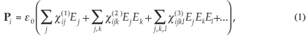
where Pi is the ith component of the polarisation induced by an electric field, Ei is the electric field component and χn the nth-order optical susceptibility tensors. If an electric field exists in the region of irradiation, this electric field can directly contribute to the generated SH signal. Second harmonic generation has been shown to be a very sensitive probe for these internal electric fields. This is referred to as electric field induced second harmonic (EFISH) generation.2,5–8,10 In the presence of an electric field (which in general is time dependent, and in this case is a result of the irradiation itself), the generated second harmonic intensity is time dependent and it can be expressed as:
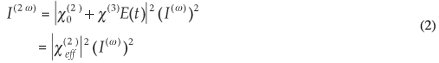
with I(w) being the incident laser intensity, E(t) the electric field that is induced in the area of irradiation, χ0(2) and χ(3) are the interfacial second- and third-order optical susceptibilities respectively, and χeff(2) is the effective photoinduced second-order optical susceptibility. It should be noted that the equilibrium second harmonic signal is a direct measure of the total trapped charge density, nc, which is responsible for the interfacial electric field10,11:

Second harmonic experimental setup
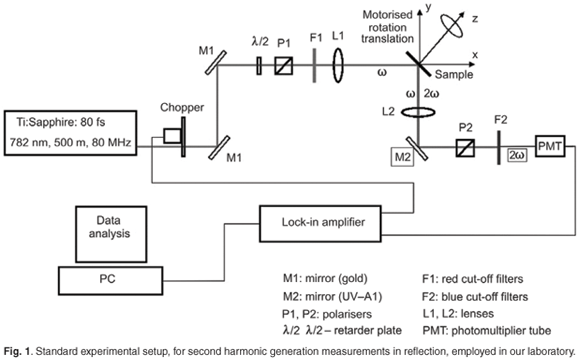
In order to probe the Si/SiO2 interface by means of optical second harmonic generation, a standard setup for measuring second harmonic generated light in reflection was used. The setup is depicted in Fig. 1. The incident laser beam was directed onto the sample at an angle of 45°. The SHG was detected in reflection at 45°. The generated SH signal was then first separated from the fundamental by a suitable set of filters, before being detected by a photomultiplier tube (PMT). The signal from the PMT was fed into a lock-in amplifier, which, together with the light chopper, ensured a good signal to noise ratio. The sample was placed on a XY-translation stage for positioning and imaging purposes. A stepper motor was also connected to enable the rotation of the sample around the azimuthal angle.
Experiment and results
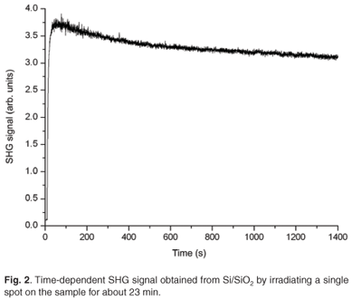
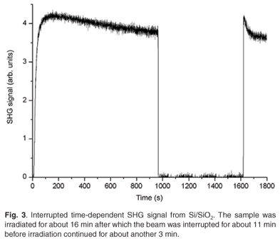
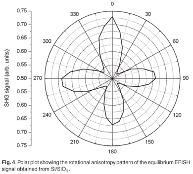
Figure 2 shows the time-dependent SHG signal from Si under femtosecond irradiation. The Si sample was irradiated at one position for approximately 23 min while the SHG signal was recorded. The signal shows a quick initial increase followed by a slow decrease until an equilibrium value is reached after several minutes of irradiation. A similar experiment was conducted to obtain Fig. 3, except that the irradiation was interrupted after about 16 min for a period of about 11 min, after which the irradiation was continued for about another 3 min. The same initial trend as in Fig. 2 can be seen in Fig. 3. After the interruption, once the irradiation was continued, the SHG signal immediately (faster than the experimental time resolution of 0.2 s) reached a maximum value followed by a quick decline in signal strength until the equilibrium value was again reached. Figure 4 is a measurement of the rotational anisotropy of the SHG signal from the Si/SiO2 system once the equilibrium electric field had been reached. It was obtained by irradiating the sample on a virgin spot until an equilibrium value was reached. This equilibrium value was then recorded. The sample was then rotated 9° around the azimuth before being irradiated again till equilibrium was reached. This procedure was repeated 40 times to obtain the full (360°) rotational anisotropy of the equilibrium EFISH signal.
Discussion
The SHG signal shows a time dependence (Fig. 2), which has been reported earlier2,5,6 and which can be explained by the creation and subsequent population of the trap sites. The creation of the trap sites as well as the population of the trap sites is a result of multi-photon absorption of the incident laser radiation. This charge separation resulted in an electric field across the interface, which contributed to the effective photoinduced second-order optical susceptibility. Eventually a constant SHG signal was obtained during irradiation, indicating that eventually an equilibrium electric field was attained.
The trap sites were created for both holes and electrons.2 The electron trap sites were populated via a three photon process under near infrared irradiation (1.59 eV, 782 nm).2 The hole trap sites required a four photon process2 to be populated, explaining why the electron dynamics occurred on a much accelerated time scale to that of the holes. It also explains why hole effects became significant only at very high peak intensities (>45 GW cm–2).2 The process of creating trap sites was significantly longer than the process of populating the trap sites. This was illustrated by the fact that after blocking the laser, the SHG signal rapidly reached equilibrium (Fig. 3).
The defects that were generated exist either in the SiO2 or in the interface layer between the oxide and the Si substrate,2,9 depending on the process by which the defect was generated. The defects created in the system were permanent and could still be detected weeks after they were generated.2 This was achieved by irradiating the defects and, since the existing trap sites were populated by electrons injected at a faster rate than at sites where fewer defects existed, resulted in the accelerated SHG response. The defects were also well localised and the influence on the SHG signal was limited to the affected area.2 The defects were created by the breaking and reforming of bonds in the SiO2, and it was possible to image them using a scanning electron microscope.2 The defects could also be imaged with SHG imaging techniques2 as the areas that contained defects showed an accelerated SHG response compared to those areas with no defects.
The fact that no SH signal originated from the bulk of the Si substrate due to symmetry considerations in the electric dipole approximation,1,12–15 implies that the SH signal originated only from the interface where the electric field existed. The anisotropy due to the electric field could be measured (Fig. 4), showing four-fold symmetry, indicating that the SHG response was due only to the presence of the electric field across the interface. This implies that the technique was able to probe an interfacial electric field as a result of populated defects that existed in a sub-5-nm region in the one dimension. This implies that SHG was able to probe electric fields originating from 'nanosized' sources.
Future research
Further research into the Si/SiO2 interface is being conducted by this laboratory, with the focus now shifted to doped Si, which implies that an internal electric field already exists across the interface as a result of the dopants. The pre-existing electric field contributes to the SH signal in the same fashion as the electric field generated by trapped electrons and holes. The SH signal can thus be taken as a direct measure of the effect of doping on a Si sample.
A future project will also look at thin films of Si, covered with native oxide. This should yield information on how the electric field that is generated across the interface interacts with the bulk of the Si to influence the SH signal.
Summary
Work done in our laboratory has shown that it is possible to probe and create electronic defects in the Si/SiO2 interface. These defects can be populated by near infrared femtosecond radiation and the effect of the defect population can be measured by optical second harmonic generation. It has also been shown that it is possible to measure the rotational anisotropy of the generated electric field. The defects generated were very localised and confined to a sub-5-nm region in one dimension. It has thus been shown that it is possible to create and populate electronic trap sites in a well-confined area, with one dimension being on the nanometre scale.
1. Lüpke G. (1999). Characterization of semiconductor interfaces by second-harmonic generation. Surf. Sci. Rep. 35, 75–161. [ Links ]
2. Scheidt T., Rohwer E.G., von Bergmann H.M. and Stafast H. (2004). Charge-carrier dynamics and trap generation in native Si/SiO2 interfaces probed by optical second-harmonic generation. Phys. Rev. B 69, 165314–165321. [ Links ]
3. Scheidt T., Rohwer E.G., von Bergmann H.M. and Stafast H. (2005). Femtosecond laser diagnostics of thin films, surfaces, and interfaces. S. Afr. J. Sci. 101 (5–6), 267–271. [ Links ]
4. Lu Z-Y., Nicklaw C.J., Fleetwood D.M., Schrimpf R.D. and Pantelides S.T. (2002). Structure, properties, and dynamics of oxygen vacancies in amorphous SiO2. Phys. Rev. Lett. 89, 285505. [ Links ]
5. Mihaychuk J.G., Bloch J. and van Driel H.M. (1995). Time-dependent second-harmonic generation from the Si–SiO2 interface induced by charge transfer. Opt. Lett. 20, 2063. [ Links ]
6. Scheidt T., Rohwer E.G., von Bergmann H.M. and Stafast H. (2005). Optical second harmonic generation as a probe for internal electric fields at the Si/SiO2 interface. S. Afr. J. Sci. 101(1–2), 91–92. [ Links ]
7. Aktsipetrov O.A., Fedyanin A.A., Golovkina V.N. and Murzina T.V. (1994). Optical second-harmonic generation induced by a dc electric field at the Si–SiO2 interface. Opt. Lett. 19, 1450–1451. [ Links ]
8. Bloch J., Mihaychuk J.G. and van Driel H.M. (1996). Electron photoinjection from silicon to ultrathin SiO2 films via ambient oxygen. Phys. Rev. Lett. 77, 920. [ Links ]
9. Scheidt T., Rohwer E.G., von Bergmann H.M. and Stafast H. (2006). Ultraviolet pulse laser induced modifications of native silicon/silica interfaces analyzed by optical second harmonic generation. J. Appl. Phys. 100(2), 023118. [ Links ]
10. Mihaychuk J.G., Shamir N. and van Driel H.M. (1999). Multiphoton photoemission and electric-field-induced optical second-harmonic generation as probes of charge transfer across the Si/SiO2 interface. Phys. Rev. B 59, 2164. [ Links ]
11. Cernusca M., Heer R. and Reider G.A. (1998). Photoinduced trap generation at the Si–SiO2 interface. Appl. Phys. B 66, 367–370. [ Links ]
12. Bloembergen N., Chang R.K., Jha S.S. and Lee C.H. (1968). Optical second-harmonic generation in reflection from media with inversion symmetry. Phys. Rev. 174, 813–822. [ Links ]
13. Sipe J.E., Moss D.J. and van Driel H.M. (1997). Phenomenological theory of optical second- and third-harmonic generation from cubic centrosymmetric crystals. Phys. Rev. B 35, 1129–1141. [ Links ]
14. Shen Y.R. (1984). The Principles of Nonlinear Optics, chap. 7, p. 93. Wiley, New York. [ Links ]
15. Boyd R.W. (1992). Nonlinear Optics, chap. 1, pp. 41–42. Academic Press, London. [ Links ]
Received 18 May. Accepted 5 June 2009.
* Author for correspondence E-mail: pietern@sun.ac.za

