


Services on Demand
Article
 English (pdf)
 Article in xml format
 Article references
Indicators

Related links
-
 Cited by Google
 -
 Similars in Google
Share

 Permalink
South African Journal of Science
On-line version ISSN 1996-7489
Print version ISSN 0038-2353
S. Afr. j. sci. vol.104 n.9-10 Pretoria Sep./Oct. 2008
RESEARCH LETTERS
Photoluminescence properties of SiO2 surface-passivated PbS nanoparticles
M.S. DhlaminiI, *; J.J. TerblansI; R.E. KroonI; O.M. NtwaeaborwaI; J.M. NgaruiyaI; J.R. BothaII; H.C. SwartI, *
IDepartment of Physics, University of the Free State, P.O. Box 339, Bloemfontein 9300, South Africa
IIDepartment of Physics, Nelson Mandela Metropolitan University, P.O. Box 77000, Port Elizabeth 6031, South Africa
ABSTRACT
SiO2:PbS nanoparticle phosphors were successfully prepared by a sol-gel process. The crystallized lead sulphide (PbS) nanoparticles inside the amorphous silicon dioxide (silica, SiO2) matrix were examined by X-ray diffraction and transmission electron microscopy (TEM) to estimate the particle size and distribution. The particles were in the size range of 10–50 nm. The TEM diffraction patterns showed the PbS particles to be cubic in structure. Two strong broad photoluminescence emission bands were observed, namely blue (450 nm) from the SiO2 matrix and yellow-orange (560 nm) from the PbS nanoparticles. In bulk PbS emission occurs at ~3200 nm, and the blue shift to the much shorter wavelength reported here is ascribed to quantum effects in the PbS nanoparticles. The emission spectra were strongly dependent on the excitation wavelength.
Introduction
Nanotechnology, which is the creation and use of materials, systems, and devices through control of matter on a nanometre-length scale, is expected to become one of the main driving forces in materials research in the present century.1 The synthesis of semiconductor nanoparticles embedded in different solid matrices is currently an active research area in nanoscience.22 It is well known that the dispersion relations for the energy of electrons and holes in a bulk semiconductor are parabolic as a first approximation as illustrated in Fig. 1(a).3,4 This approximation is true only for levels that are occupied by electrons near the bottom of the conduction (CB) and by holes near the top of the valence (VB) band, respectively. It is important to remember that these parabolas are really a quasi-continuous set of electron (hole) states along a given direction in k-space and that the lowest occupied level in the CB and the highest occupied level in the VB are separated by an energy gap, which for bulk materials is usually of the order of an electron volt. When the dimensionality of the semiconductor bulk material is reduced to a zero-dimensional quantum dot, the quasi-continuous nature is de-emphasized, as only discrete energy levels can exist in the dot.
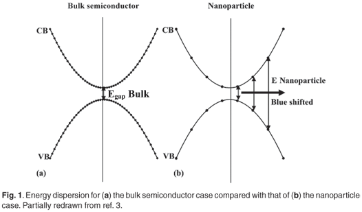
Subsequently, each of the original parabolic bands of the bulk case is fragmented into an ensemble of points for a nanoparticle as demonstrated in Fig. 1(b). These atomic-like electron energy levels are formed due to charge-carrier confinement (quantum confinement) in three dimensions and result in an increase (blue shift) of the effective band gap compared to that of the corresponding bulk materials.5–8 Accordingly, the effective band gaps of PbS nanoparticles are markedly blue-shifted from the near-infrared (~3200 nm) into the visible and near-ultraviolet region with decreasing particle size.9 The luminescence corresponding to exciton recombination in a single nanocrystal has a finite width as a result of homogeneous line broadening. Additionally, there will always be a statistical distribution of particle sizes due to the sample preparation process, and the dependence of the effective bandgap on the particle size will produce a further broadening effect as illustrated in Fig. A in supplementary material online.
Practical applications in photonics of these nanoparticles are reportedly lacking because surface-related non-radiative recombination dominates in the quantum confinement regime,10 exacerbated by the large surface to volume ratio of the particles.11 However, the non-radiative contribution from the surface states can be eliminated by passivating dangling bonds of the free-standing nanoparticles. Achieving proper surface passivation is therefore extremely important for nanoparticles, especially in the strong quantum confinement regime.12,13 This can be achieved in several ways, such as suspending them as colloidal particles in a liquid, forming nanocrystals in a matrix such as glass or polymers, or enclosing nanocrystals in cage zeolites.10–15 The photoluminescence emission from surface-passivated PbS nanoparticles can range from a deep-red to a broad yellow-white, depending on the preparation conditions.9,16
In this study, PbS nanoparticles with a median size of 17 nm embedded in an SiO2 matrix were synthesized by a sol-gel process. The structural and photoluminescence properties of the nanoparticles are presented here.
Experimental
Silica gel13 was prepared by mixing 10 g tetraethylorthosilicate (TEOS) solution and 5 g ethanol with drops of 0.15 M nitric acid (HNO3) as catalyst. The process is illustrated in Fig. B online. The mixture was stirred for 1 hour. To the resulting transparent solution, 0.03 g lead acetate trihydrate Pb(CH3COO)2.3H2O dissolved in 5 g ethanol and 0.01 g Na2S dissolved in 5 g ethanol, respectively, were separately added to form SiO2:PbS gel. The mixed solution was stirred for a further 30 minutes to complete the reaction. The gel was then dried for 10 days, after which it was ground and calcined/sintered at 200°C for 2 hours. All steps other than calcination were carried out at room temperature.
The particle size and crystalline structure of the PbS nanoparticles were determined by X-ray diffraction (XRD) and TEM. Scanning electron microscopy (SEM) was used to determine the morphology. A He-Cd laser (325 nm) and Ar+ laser (458 nm) were used to excite photoluminescence in the phosphor and the spectra were collected using a 0.5-m SPEX 1870 spectrometer.
Results and discussion
The diameter of the PbS nanoparticles prepared in this way, as calculated from the broadening of XRD spectra, was 16 ± 2 nm.17 An SEM image of the SiO2:PbS powder sample is shown in Fig. 2, which reveals multi-facets of agglomerated composite particles with nano-sized particles on the surface. Most of the particles measured about a micrometre in diameter. A TEM image was obtained from material [Fig. 3(a)] first suspended in ethanol and then allowed to dry on a carbon-covered copper grid. The black spots in the image are the crystalline PbS nanoparticles, enveloped in amorphous SiO2. Interplanar spacings calculated from the TEM diffraction pattern in Fig. 3(b) correspond well with those calculated for the standard PbS (galena) cubic crystalline structure18 (Table 1). Most of the particles were in the order of 17 nm in diameter, slightly smaller than the exciton Bohr diameter of PbS,8 but there were also smaller (10 nm) and bigger agglomerations (up to 50 nm).


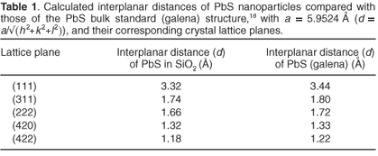
Figure 4 shows the photoluminescence (PL) emission spectrum of a pure SiO2 powder control sample (without PbS) excited at a wavelength of 325 nm. The broad emission band at 450 nm has been ascribed to the defect luminescence originating from neutral oxygen vacancies.19 Figure 5(a) presents the normalized PL spectra of the SiO2:PbS powder sample excited at wavelengths of 325 nm and 458 nm. The spectrum excited using the shorter wavelength shows a strong peak at ~450 nm, which is attributed to the SiO2 and a shoulder at ~560 nm which is attributed to the PbS nanoparticles. The longer excitation wavelength used did not provide enough energy to excite the SiO2 peak, and the spectrum using this wavelength shows only the emission peak at ~560 nm of the PbS nanoparticles. Yang et al.13 have reported PL spectra of PbS embedded in sol-gel silica glass with an emission peak at 440 nm when excited at 380 nm and another peak at 605 nm when excited at 475 nm. In their study, no shoulder was observed when they excited at 380 nm and the same emission wavelength (440 nm) was observed for the pure sol-gel silica glass. Sashchiuk et al.7 reported a broad emission band of PbS in the range of 600–800 nm in their study of optical and conductivity properties of PbS nanocrystals embedded in amorphous zirconia. A broad PL emission band peaking at 804 nm was observed also by Chen et al.2 for alkanethiolate-capped PbS nanoparticles. Cao et al.9 observed a broad PL emission at 434 nm in their study of the growth and PL properties of PbS nanocubes. For PbS nanoparticles coated with CdS, a broad band emission peak at 510 nm was observed by Warner et al.20 Our results show some similarities and also differences from previous studies. The difference can be ascribed to the different reaction environments and contrasting host materials. The luminescence properties of PbS can therefore be affected by host materials, depending on the reaction conditions.

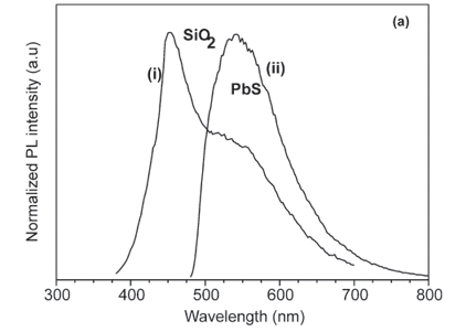
The spectra in Fig. 5(a) show that the luminescence peak ascribed to the PbS nanoparticles is not symmetrical, but has a tail towards longer wavelengths. To investigate this, the spectrum excited at 325 nm was fitted with multiple Gaussian profiles. Figure 5(b) shows that three Gaussian peaks are necessary to provide an acceptable fit, with peak wavelengths of 450 nm (corresponding to the SiO2 emission), 514 and 593 nm. The latter two wavelengths correspond to different transitions from the PbS. The possible allowed electronic transitions in nanoparticles for exciton recombination are schematically illustrated in Fig. C online and designated by Se–Sh and Pe–Ph. Based on the possible energy levels of an electron confined in a quantum dot, if the bandgap energy is negligible compared with the confinement energy as is the case here, then the Pe–Ph transition should have double the energy (i.e. half the wavelength) of the Se–Sh transition. We note that this is indeed true for the measurements of Warner et al.,20 although their ascribing an emission at intermediate wavelength to a Se–Ph transition is questionable because this is not an allowed transition. In our case, the wavelengths of 514 and 593 nm cannot be ascribed to these different transitions. Rather, the shorter wavelength emission is ascribed to a direct recombination and the longer wavelength to a recombination through shallow surface states.11,16,21,22

Conclusion
PbS nanoparticles with polyhedral shapes and a median size of ~17 nm were successfully prepared using a sol-gel method. Analysis of a TEM electron diffraction pattern showed that the nanoparticles were crystalline and the interplanar spacings compared well with those of the standard galena structure. To get the PbS nanoparticles to luminesce, for possible photonic applications, their surfaces must be passivated to avoid non-radiative recombinations. This was achieved by incorporating the nanoparticles in an SiO2 matrix during the sol-gel preparation process. The observed photoluminescence was due to both the PbS nanoparticles and the SiO2 matrix. The emission from the former occurred in the visible wavelength range, and consisted of two separate broad overlapping peaks centred on 514 and 593 nm. Emission from bulk PbS occurs in the infrared, so that a significant blue-shifting occurred due to the quantum confinement effect, which was expected because the diameter of the nanoparticles was slightly less than the exciton Bohr diameter of bulk PbS. The emission of the PbS nanoparticles can therefore be changed by altering their size. The broadness of the peaks can be ascribed to the variation in particle size produced by the sol-gel process. In some applications the emissions from the SiO2 matrix may be undesirable, so future work should include the investigation of other matrix materials.
This work was supported by the National Research Foundation and the Council for Scientific and Industrial Research. We thank P.W.J. van Wyk from the Centre of Confocal and Electron microscopy, University of the Free State, for the SEM and TEM measurements. J.R.B. acknowledges that this work is based on research supported by the South African Research Chairs Initiative of the Department of Science and Technology and the National Research Foundation.
1. Rogach A.L., Eychmuller A., Hickey S.G. and Kershaw S.V. (2007). Infrared-emitting colloidal nanocrystals: Synthesis, assembly, spectroscopy, and applications. Small. Online at: www.small-journal.com. 3(4), 536–557. [ Links ]
2. Chen S., Truax L.A. and Sommers J.M. (2000). Alkanethiolate-protected PbS nanoclusters: Synthesis, spectroscopic and electrochemical studies. Chem. Mater. 12, 3864–3870. [ Links ]
3. Parak W.J., Manna L., Simmel F.C., Gerion D. and Alivisatos A.P. (2004). Nanoparticles—From Theory to Applications, ed. G. Schmid, pp. 17–18. Wiley–VCH Verlag, KGaA, Weinheim. [ Links ]
4. Machol J.L., Wise F.W. , Patel R.C. and Tanner D.B. (1993). Vibronic quantum beats in PbS microcrystallites. Phys. Rev. B 48(4), 2819–2822. [ Links ]
5. Naves P.M., Gonzaga T.N., Monte A.F.G. and Dantas N.O. (2006). Band gap energy of PbS quantum dots in oxide glasses as a function of concentration. J. Non-Crystal. Solids 352, 3633–3635. [ Links ]
6. Tang H., Xu G., Weng L., Pan L. and Wang L. (2004). Luminescence and photophysical properties of colloidal ZnS nanoparticles. Acta Mater. 52, 1489–1494. [ Links ]
7. Sashchiuk A. and Lifshitz E. (2002). Optical and conductivity properties of PbS nanocrystals in amorphous zirconia sol-gel films. J. Sol-Gel Sci. Technol. 24(1), 31–38. [ Links ]
8. Patel A.A., Wu F., Zhang J.Z., Torres-Martinez C.L., Mehra R.K., Yang Y. and Risbud S.H. (2000). Synthesis, optical spectroscopy and ultrafast electron dynamics of PbS nanoparticles with different surface capping. J. Phys. Chem. B 104, 11598–11605. [ Links ]
9. Cao H., Wang G., Zhang S. and Zhang X. (2006). Growth and photoluminescence properties of PbS nanocubes. Nanotechnology 17(13), 3280–3287. [ Links ]
10. Bhargava R.N. (1996). Doped nanocrystalline materials – Physics and applications. J. Lumin. 70, 85–94. [ Links ]
11. Fernee M.J., Watt A., Warner J., Cooper S., Heckenberg N. and Rubinsztein-Dunlop H. (2003). Inorganic surface passivation of PbS nanocrystals resulting in strong photoluminescent emission. Nanotechnology 14(9), 991–997. [ Links ]
12. Fernee M.J., Thomsen E., Jensen P. and Rubinsztein-Dunlop H. (2006). Highly efficient luminescence from a hybrid state found in strongly quantum confined PbS nanocrystals. Nanotechnology 17(4), 956–962. [ Links ]
13. Yang P., Song C.F., Lu M.K., Yin X., Zhou G.J., Xu D. and Yuan D.R. (2001). The luminescence of PbS nanoparticles embedded into sol-gel silica glass. Chem. Phys. Lett. 345, 429–434. [ Links ]
14. Lifshitz E., Sirota M. and Porteanu H. (1999). Continuous and time-resolved photoluminescence study of lead sulfide nanocrystals, embedded in polymer film. J. Crystal Growth 196(1), 126–134. [ Links ]
15. Lippens P.E. and Lannoo M. (1991). Optical properties of II–VI semiconductor nanocrystals. Semicond. Sci. Technol. 6, A157–A160 [ Links ]
16. Fernee M.J., Watt A., Warner J., Cooper S., Heckenberg N. and Rubinsztein-Dunlop H. (2004). Evidence for energy relaxation via a radiative cascade in surface-passivated PbS quantum dots. Nanotechnology 15(9), 1328–337. [ Links ]
17. Dhlamini M.S., Terblans J.J., Ntwaeaborwa O.M., Joubert H.D. and Swart H.C. (2008). Preparations and luminescent properties of PbS nanoparticle phosphors incorporated in a SiO2 matrix. Phys. Stat. Sol. C 5, 598–01. [ Links ]
18. Kumar S., Khan M.A.M., Khan S.A. and Husain M. (2004). Studies on vacuum evaporated PbS1–xSex thin films. Opt. Mat. 25(1), 25–32. [ Links ]
19. Inokuma T., Kurata Y. and Hasegawa S. (1999). Cathodoluminescence properties of silicon nanocrystallites embedded in silicon oxide thin films. J. Lumin. 80, 247–251. [ Links ]
20. Warner J.H. , Watt A.R., Fernee M.J., Heckenberg N.R. and Rubinsztein-Dunlop H. (2005). Separating fluorescent species of aqueous PbS semiconductor nanocrystals using micro-emulsions. Nanotechnology 16(4), 479–483. [ Links ]
21. Capoena B., Martuccib A., Turrellb S. and Bouazaoui M. (2003). Effects of the sol-gel solution host on the chemical and optical properties of PbS quantum dots. J. Mol. Struct. 651, 467–473. [ Links ]
22. Fernee M.J., Watt A., Warner J., Heckenberg N. and Rubinsztein-Dunlop H. (2004). Direct observation of mixed-parity excited states in surface-passivated PbS nanocrystals. Nanotechnology 15(9), 1351–1355. [ Links ]
Received 8 August. Accepted 14 October 2008.
This article is accompanied by supplementary figures online at www.sajs.co.za
* Authors for correspondence. E-mail: swarthc.sci@ufs.ac.za or dhlaminims.sci@ufs.ac.za.
Dhlamini M.S., Terblans J.J., Kroon R.E., Ntwaeaborwa O.M. Ngaruiya J.M., Botha J.R. and Swart H.C. (2008). Photoluminescence properties of SiO2 surface-passivated PbS nanoparticles. S. Afr. J. Sci. 104, 398–400.


